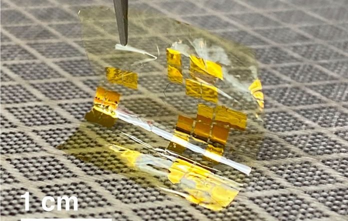
New, ultrathin photovoltaic materials could eventually be used in mobile applications, from self-powered wearable devices and sensors to lightweight aircraft and electric vehicles.
A race is on in solar engineering to create almost impossibly-thin, flexible solar panels. Engineers imagine them used in mobile applications, from self-powered wearable devices and sensors to lightweight aircraft and electric vehicles.
Against that backdrop, researchers at Stanford University have achieved record efficiencies in a promising group of photovoltaic materials.
Chief among the benefits of these transition metal dichalcogenides—or TMDs—is that they absorb ultrahigh levels of the sunlight that strikes their surface compared to other solar materials.
“Imagine an autonomous drone that powers itself with a solar array atop its wing that is 15 times thinner than a piece of paper,” said Koosha Nassiri Nazif, a doctoral scholar in electrical engineering at Stanford and co-lead author of a study published in Nature Communications.
“That is the promise of TMDs.”
The search for new materials is necessary because the reigning king of solar materials, silicon, is much too heavy, bulky and rigid for applications where flexibility, lightweight and high power are preeminent, such as wearable devices and sensors or aerospace and electric vehicles.
“Silicon makes up 95 percent of the solar market today, but it’s far from perfect. We need new materials that are light, bendable and, frankly, more eco-friendly,” said Krishna Saraswat, a professor of electrical engineering and senior author of the paper.
A competitive alternative
While TMDs hold great promise, research experiments to date have struggled to turn more than 2 percent of the sunlight they absorb into electricity. For silicon solar panels, that number is closing in on 30 percent.
To be used widely, TMDs will have to close that gap.
The new Stanford prototype achieves 5.1 percent power conversion efficiency, but the authors project they could practically reach 27 percent efficiency upon optical and electrical optimizations. That figure would be on par with the best solar panels on the market today, silicon included.
Moreover, the prototype realized a 100-times greater power-to-weight ratio of any TMDs yet developed. That ratio is important for mobile applications, like drones, electric vehicles and the ability to charge expeditionary equipment on the move.
When looking at the specific power—a measure of electrical power output per unit weight of the solar cell—the prototype produced 4.4 watts per gram, a figure competitive with other current-day thin-film solar cells, including other experimental prototypes.
“We think we can increase this crucial ratio another ten times through optimization,” Saraswat said, adding that they estimate the practical limit of their TMD cells to be a remarkable 46 watts per gram.
Additional advantages
Their biggest benefit, however, is their remarkable thinness, which not only minimizes the material usage and cost but also makes TMD solar cells lightweight and flexible and capable of being molded to irregular shapes—a car roof, an airplane wing or the human body.
The Stanford team was able to produce an active array that is just a few hundred nanometers thick. The array includes the photovoltaic TMD tungsten diselenide and contacts of gold spanned by a layer of conducting graphene that is just a single atom thick.
All that is sandwiched between a flexible, skin-like polymer and an anti-reflective coating that improves the absorption of light.
When fully assembled, the TMD cells are less than six microns thick—about that of a lightweight office trash bag. It would take 15 layers to reach the thickness of a single piece of paper.
While thinness, lightweight and flexibility are all highly desirable goals in and of themselves, TMDs present other engineering advantages as well.
They are stable and reliable over the long term. And unlike other challengers to the thin-film crown, TMDs contain no toxic chemicals. They are also biocompatible, so they could be used in wearable applications requiring direct contact with human skin or tissue.
A promising future
The many advantages of TMDs are countered by certain downsides, mostly in the engineering intricacies of mass production.
The process of transferring an ultrathin layer of TMD to a flexible, supporting material often damages the TMD layer.
Alwin Daus, who was co-lead author on the study with Nassiri Nazif, devised the transfer process that affixes the thin TMD solar arrays to the flexible substrate. He said this technical challenge was considerable.
One step involved transferring the layer of atomically thin graphene onto a flexible substrate that is just a few microns thick, explained Daus, who was a postdoctoral scholar in Eric Pop’s research group at Stanford when the research was conducted. He is now a senior researcher at RWTH Aachen University in Germany.
This intricate process results in the TMD being fully embedded in the flexible substrate leading to greater durability. The researchers tested the flexibility and robustness of their devices by bending them around a metal cylinder less than a third of an inch thick.
“Powerful, flexible and durable, TMDs are a promising new direction in solar technology,” Nassiri Nazif concluded.
Written by Andrew Myers.


