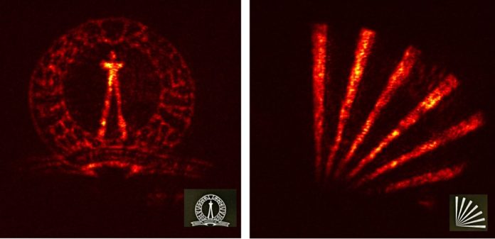
The human eye can only see light within a specific range of frequencies known as the visible spectrum, with red light being the lowest. Infrared light, which is invisible to us, has an even lower frequency.
Researchers at the Indian Institute of Science (IISc) have now created a device that can convert, or “up-convert,” infrared light to visible light.
This breakthrough has numerous applications, particularly in defense and optical communications.
For the first time, the IISc team used a 2D material to design a non-linear optical mirror stack to achieve this up-conversion, combined with widefield imaging capability.
The stack is made of multiple layers of gallium selenide on top of a gold reflective surface, with a layer of silicon dioxide in between.
Traditional infrared imaging uses specialized low-energy bandgap semiconductors or micro-bolometer arrays to detect heat or absorption signatures.
Infrared imaging is valuable in fields ranging from astronomy to chemistry. For instance, when infrared light passes through a gas, analyzing the light changes can reveal specific properties of the gas, something not always possible with visible light.
However, existing infrared sensors are bulky, inefficient, and often restricted for export due to their military applications.
Therefore, there is a critical need for efficient, locally developed devices.
The IISc team’s method involves feeding an input infrared signal along with a pump beam onto the mirror stack. The nonlinear optical properties of the stack’s material mix the frequencies, producing an output beam with an increased (up-converted) frequency while preserving the original properties.
Using this method, they successfully up-converted infrared light with a wavelength of around 1550 nm to visible light at 622 nm. The output light can be detected using standard silicon-based cameras.
“This process is coherent, meaning the properties of the input beam are preserved in the output. If a particular pattern is imprinted in the input infrared frequency, it automatically transfers to the new output frequency,” explains Varun Raghunathan, Associate Professor in the Department of Electrical Communication Engineering (ECE) and corresponding author of the study published in Laser & Photonics Reviews.
Gallium selenide was chosen for its high optical nonlinearity, allowing a single photon of infrared light and a single photon of the pump beam to combine into a single photon of up-converted light.
The team achieved up-conversion with a thin layer of gallium selenide measuring just 45 nm, making it more cost-effective than traditional devices that use centimeter-sized crystals. Its performance is comparable to current state-of-the-art up-conversion imaging systems.
Jyothsna K Manattayil, a Ph.D. student at ECE and the first author, explains that they used a particle swarm optimization algorithm to determine the optimal layer thickness. Depending on the thickness, different wavelengths can pass through gallium selenide and be up-converted. This requires adjusting the material thickness based on the application.
“In our experiments, we used infrared light of 1,550 nm and a pump beam of 1,040 nm. But the device can work for other wavelengths too,” she says. “We saw good performance across a range of infrared wavelengths from 1,400 nm to 1,700 nm.”
The researchers plan to extend their work to up-convert light of longer wavelengths and improve the device’s efficiency by exploring other stack geometries.
“There is a lot of global interest in infrared imaging without infrared sensors. Our work could be a gamechanger for these applications,” says Raghunathan.
Source: KSR.


