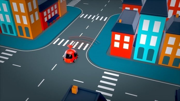
You’re in an autonomous car when a rabbit suddenly hops onto the road in front of you.
Here’s what typically happens: the car’s sensors capture images of the rabbit; those images are sent to a computer where they are processed and used to make a decision; that decision is sent to the car’s controls, which are adjusted to safely avoid the rabbit.
Crisis averted.
This is just one example of computer vision—a field of AI that enables computers to acquire, process, and analyze digital images, and make recommendations or decisions based on that analysis.
The computer vision market is growing rapidly and includes everything from DoD drone surveillance to commercially available smart glasses, to rabbit-avoiding autonomous vehicle systems.
Because of this, there is increased interest in improving the technology.
Researchers at USC Viterbi’s Information Sciences Institute (ISI) and the Ming Hsieh Department of Electrical and Computer Engineering (ECE) have recently completed Phases 1 and 2 of a DARPA (Defense Advanced Research Projects Agency) project looking to make advances in computer vision.
Two jobs spread over two separate platforms
In the rabbit-in-the-road scenario above, on the “front end” is the vision sensing (where the car’s sensors capture the rabbit’s image) and on the “back end” is the vision processing (where the data is analyzed).
These are conducted on different platforms, which are traditionally physically separated.
Ajey Jacob, Director of Advanced Electronics at ISI explains the effect of this: “In applications requiring large amounts of data to be sent from the image sensor to the backend processors, physically separated systems and hardware lead to bottlenecks in throughput, bandwidth and energy efficiency.”
In order to avoid that bottleneck, some researchers approach the problem from a proximity standpoint—studying how to bring the backend processing closer to the frontend image collection. Jacob explained this methodology.
“You can bring that processing onto a CPU [computer] and place the CPU closer to the sensor. The sensor is going to collect the information and send it to the computer. If we assume this is for a car, it’s fine. I can have a CPU in the car to do the processing.
However, let’s assume I have a drone. I cannot take this computer inside the drone because the CPU is huge. Plus, I’ll need to make sure that the drone has an Internet connection and a battery large enough for this data package to be sent.”
So the ISI/ECE team took another approach, and looked at reducing or eliminating the backend processing altogether.
Jacob states, “What we said is, let’s do the computation on the pixel itself. So you don’t need the computer. You don’t need to create another processing unit. You do the processing locally, on the chip.”
Front-end processing inside a pixel
Processing on the image sensor chip for AI applications is known as in-pixel intelligent processing (IP2). With IP2, the processing occurs right under the data on the pixel itself, and only relevant information is extracted.
This is possible thanks to advances in computer microchips, specifically CMOS (complementary metal–oxide–semiconductors), which are used for image processing.
The team has proposed a novel IP2 paradigm called processing-in-pixel-in-memory (P2M) which leverages advanced CMOS technologies to enable the pixel array to perform a wider range of complex operations—including image processing.
Akhilesh Jaiswal, a computer scientist at ISI and assistant professor at ECE, led the front-end circuit design. He explained, “We have proposed a new way of fusing together sensing, memory and computing within a camera chip by combing, for the first time, advances in mixed signal analog computing and coupling them with strides being made in 3D integration of semiconductor chips.”
After processing in-pixel, only the compressed meaningful data is transmitted downstream to the AI processor, significantly reducing power consumption and bandwidth. “A lot of work went into figuring out the right trade-off between compression and computing on the pixel sensor,” said Joe Mathai, senior research engineer at ISI.
After analyzing that trade-off, the team created a framework that reduces the chip to the size of a sensor. And the data that is transferred from the sensor to the computer is also very small, because data is first pruned, or computed on the pixel itself.
From the front to the back and into the future
RPIXELS (Recurrent Neural Network Processing In-Pixel for Efficient Low-energy Heterogeneous Systems) is the resulting proposed solution for the DARPA challenge.
It combines the front-end in-pixel processing with a back end that the ISI team has optimized to support the front.
In testing the RPIXEL framework, the team has seen promising results: a reduction in both data size and bandwidth of 13.5x (the DARPA goal was 10x reduction of both metrics).
ISI senior computer scientist Andrew Schmidt said, “RPIXELS reduces both the latency (time taken to do the image processing) and needed bandwidth by tightly coupling the fist layers of a neural network directly into the pixel for computing.
This allows for faster decisions to be made based on what is ‘seen’ by the sensor. It also enables researchers to develop novel back end object detection and tracking algorithms to continue to innovate for more accurate and higher performance systems.”
“This project is a wonderful example of collaboration between the USC ECE department and ISI,” said Peter Bereel, Professor of Computer and Electrical Engineering at ECE.
“We’ve mixed ECE’s expertise at the boundary between hardware and machine learning algorithms with the device, circuit and machine learning application expertise at ISI.”
The next step is to create a physical chip by putting the circuit onto a silicon and testing it in the real world, which could, among other things, save some rabbits.


