A research team has made significant progress in the field of two-dimensional (2D) electrical devices by developing an innovative technique that improves the contact between 2D materials and metal electrodes.
This advancement, published in Nature Communications, could lead to better-performing and more reliable 2D electronic devices.
Traditionally, creating 2D electrical devices involves a critical step where metal electrodes are deposited onto the surface of 2D materials.
However, this process often damages the delicate lattices of the 2D materials, which negatively affects the device’s electrical performance.
Reliable contact between 2D materials and metal electrodes is essential to overcome this issue.
Recent studies have highlighted the potential of van der Waals (vdW) contacts for 2D electronic devices. vdW contact refers to the interaction between 2D materials and metal electrodes through vdW forces, avoiding the introduction of defects and ensuring good electrical contact.
This method holds promise for large-scale applications.
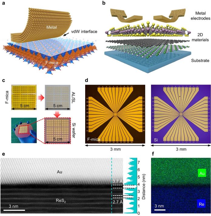
The research team developed an all-stacking technique to achieve reliable 2D vdW contacts. This technique involves directly stacking metal electrodes onto 2D materials during device fabrication, eliminating the need for metal deposition.
This protects the 2D materials from damage and enhances electrical performance.
Using this technique, the team fabricated 2D electrical devices with sharp metal-semiconductor contact interfaces, smooth vdW gaps, and no metal atom doping on the 2D material side. These features indicate the formation of high-quality vdW contact between the metal electrodes and the 2D semiconductor.
As a result of the improved contact interface, 2D semiconductor transistors created using this technique showed a more than 95% reduction in off-state current and a 50% decrease in subthreshold swing compared to those made using metal deposition processes.
They also had a higher on-off ratio, making them more suitable for low-power integrated circuits.
To demonstrate the potential for large-scale manufacturing, the team used this technique to create an array of field-effect transistors based on monolayer molybdenum disulfide. The device yield was an impressive 98.4%, with excellent consistency and stability.
The average on-off ratio of the transistor array was 6.8×10⁶, with 91.3% of the devices having an on-off ratio greater than 10⁶. This high performance and consistency showcase the advantages of the all-stacking technique for 2D electronic devices.
Led by Professors Zeng Hualing, Qiao Zhenhua, and Shao Xiang from the University of Science and Technology of China (USTC), this research offers a new, efficient, and high-quality approach for the preparation of 2D electronic devices.
It is expected to pave the way for industrial-level manufacturing of future 2D electronic devices.


