Scientists studying ultra-thin semiconductor materials have made a surprising discovery that could change the way we design electronic devices, from lasers to future quantum computers.
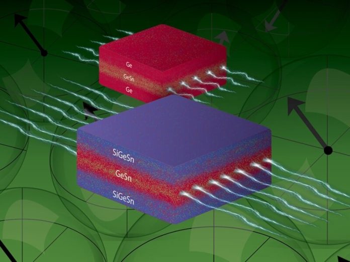
The work focuses on a structure called a quantum well—a layer only a few atoms thick—made of germanium-tin (GeSn) and sandwiched between barriers of silicon-germanium-tin (SiGeSn). Researchers expected electrical charges to move more slowly through this structure.
Instead, they found the opposite: the charges moved faster.
This unexpected result comes from a collaboration between the University of Arkansas, Sandia National Laboratories and Dartmouth College.
The study, published in Advanced Electronic Materials, suggests that tiny differences in how atoms arrange themselves may be key to improving the speed and efficiency of next-generation electronic devices.
A quantum well can be imagined like a marble rolling in a narrow groove. The marble can only move along the groove, not sideways.
In the same way, a quantum well restricts the movement of electrons and “holes,” which are the empty spots electrons can fill.
Because motion is limited, electrons behave more predictably, and this predictable behavior is used to design lasers, infrared detectors, solar cells and fast computer chips.
The ease with which electrons move through the well is called mobility, and higher mobility usually means better performance.
For years, scientists typically studied GeSn quantum wells surrounded by pure germanium barriers.
The new study instead used barriers made from a mixture of silicon, germanium and tin. This mixture is attractive because it matches better with silicon—the foundation of almost all modern electronics. However, researchers assumed the mixed barriers would slow things down because adding extra elements normally disrupts electron flow.
But when Sandia tested the devices, mobility turned out to be higher than expected. That meant electrons could move more easily through the quantum well, opening the door to faster and more efficient electronics. The big question was: why?
The answer may lie in a concept called short-range ordering. Until recently, scientists didn’t know whether small amounts of added elements—like silicon or tin—were arranged randomly or followed a subtle pattern inside the material.
New research from Lawrence Berkeley National Laboratory and George Washington University showed that atoms do form these tiny, consistent patterns. Yu and his collaborators were part of that discovery.
If atoms in the SiGeSn barriers arrange themselves in a structured pattern rather than scattering randomly, they may actually create a smoother path for electrons, increasing mobility. This could explain the surprising results and suggests that controlling this atomic ordering might let scientists design materials with dramatically better performance.
Researchers say this discovery gives engineers a new “tool” for shaping future technologies. By manipulating atomic arrangements on a nanometer scale—where millions of atoms still fit—they may be able to build faster microchips, more efficient sensors and even devices that support neuromorphic and quantum computing.
According to Yu, the findings show how much room there is to improve materials when scientists can guide atoms into the right positions. This breakthrough could mark an exciting shift in how we build the electronics of tomorrow.
Source: KSR.


