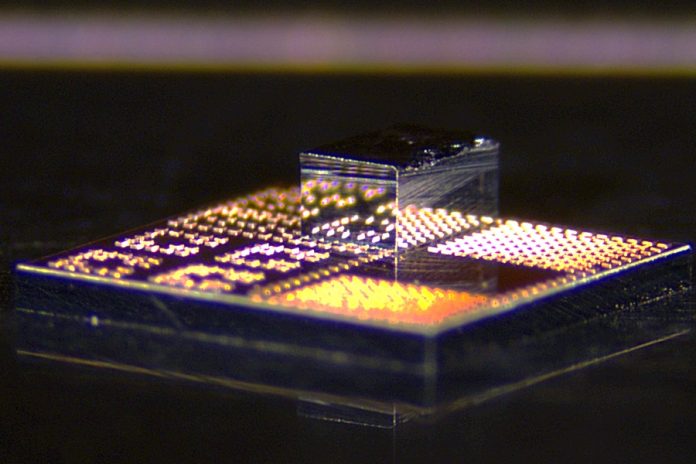
MIT engineers have found a new way to make electronics faster and more energy-efficient using a powerful material called gallium nitride (GaN).
While GaN can outperform traditional silicon chips—especially for high-speed communication and power-hungry devices—it’s been too expensive and hard to use widely.
But now, thanks to a new fabrication method, that could be about to change.
The research team developed a technique to combine small GaN transistors directly with regular silicon chips in a way that’s low-cost, scalable, and compatible with current manufacturing systems.
The breakthrough was recently presented at a major technology conference and could impact everything from smartphones to data centers—and even future quantum computers.
Instead of using large amounts of GaN, the researchers created many tiny transistors on a GaN wafer, then cut them into small pieces, each about the size of a grain of salt. These pieces, called “dielets,” are then carefully attached to a silicon chip.
The process is done at low temperatures, so it doesn’t damage either material.
This approach has two major advantages. First, it saves money by using only a tiny amount of GaN—just enough to boost performance. Second, by spacing the GaN transistors across the silicon chip, the system runs cooler. That’s key for electronics, which often overheat when packed too tightly.
To prove it works, the team used this method to make a power amplifier—the component in your phone that boosts your signal. The result was a chip that outperformed current silicon-based devices, with better signal strength, faster speeds, and improved energy efficiency. For everyday users, this could mean clearer calls, faster downloads, better wireless connections, and longer battery life.
What makes this development even more exciting is that the new chips are made using standard industry tools. Unlike other methods that rely on expensive materials like gold or require high-heat bonding, this process uses copper, which is cheaper, safer, and more efficient. This means the technology could be adopted in existing chip factories without a complete redesign.
To build such tiny, precise systems, the team also created a special tool that uses vacuum suction to move and place each tiny transistor on the chip. The tool can align the parts with extreme accuracy, then apply just the right amount of heat and pressure to fuse them together.
Eventually, this technology could be used for advanced applications like quantum computing. GaN performs better than silicon at extremely low temperatures, which are required for quantum systems to function. So beyond improving today’s electronics, these chips could also help power the computers of the future.
MIT graduate student Pradyot Yadav, the lead author, said the goal was to combine the best parts of both materials—GaN for speed and power, and silicon for affordability and versatility. The result is a new type of hybrid chip that could dramatically change the electronics industry by offering better performance without raising costs.
Source: MIT.


