The electronics industry is facing a challenge: it’s running out of space to pack more transistors onto computer chips.
To solve this, chip manufacturers are exploring ways to stack components vertically, like building a skyscraper instead of spreading out like a ranch house.
Stacking multiple layers of semiconductors could create chips capable of handling far more data and performing more complex tasks than current technology allows.
But there’s been a major obstacle. Traditional chips are built on bulky silicon wafers, which act as the base layer.
Adding multiple layers means each one has to include a thick layer of silicon, which slows down communication between the layers.
Now, engineers at MIT have developed a new method that eliminates the need for these silicon layers, making stacked chips faster and more efficient.
The team’s breakthrough is detailed in a study published in Nature.
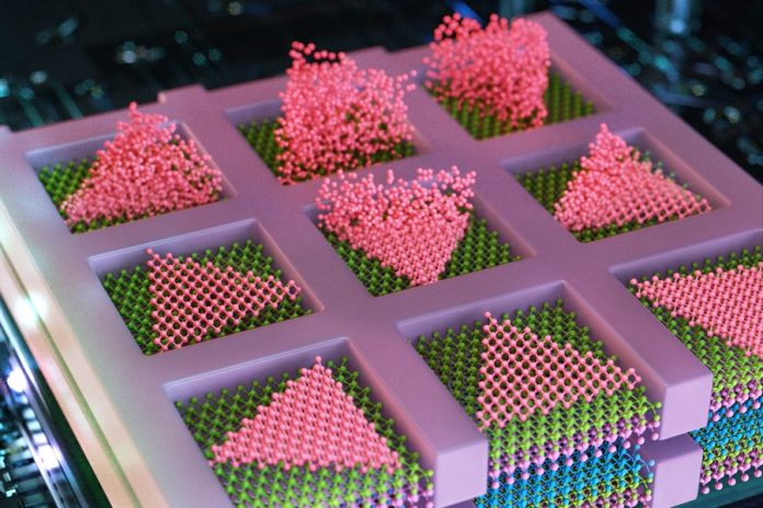
They’ve created a method to grow high-quality semiconductors directly on top of each other without requiring a silicon base. Importantly, this process works at low temperatures, preserving the delicate circuitry underneath.
This innovation could pave the way for advanced chips that power artificial intelligence (AI), wearable devices, and laptops—offering speeds and storage capacities comparable to today’s supercomputers.
“This breakthrough opens enormous possibilities for the semiconductor industry,” says Jeehwan Kim, the study’s lead author and an associate professor at MIT. “It could lead to dramatic improvements in computing power for AI, memory, and logic applications.”
In previous work, Kim’s team developed a way to grow a type of semiconductor called transition-metal dichalcogenides (TMDs), which are seen as a future replacement for silicon. TMDs maintain their semiconducting properties even at incredibly small scales, unlike silicon, which loses efficiency as it shrinks.
The challenge was to grow these materials at low temperatures—below 400°C—without damaging the underlying circuits. To solve this, the team borrowed an idea from metallurgy, the science of working with metals.
Metallurgists know that when liquid metal is poured into a mold, it forms crystals more easily at the edges. Inspired by this, the researchers deposited TMD “seeds” at the edges of tiny pockets on a silicon dioxide mask. These seeds grew into high-quality crystalline semiconductors at just 380°C.
Using this method, the team built a chip with alternating layers of two TMD materials: molybdenum disulfide for n-type transistors and tungsten diselenide for p-type transistors.
These two types of transistors are essential for creating logic circuits. By growing the layers directly on top of each other without intermediate silicon wafers, they effectively doubled the density of the chip’s components.
This new method allows for stacking tens or even hundreds of layers, enabling chips to handle far more data and communicate efficiently between layers. It also eliminates the limitations of traditional 3D chips, which require drilling holes through silicon wafers to connect layers.
To scale up this innovation, Kim has launched a company called FS2 (Future Semiconductor 2D materials). “We’ve demonstrated the concept at a small scale,” he says. “The next step is to create fully functional AI chips.”
This research, supported by Samsung and the U.S. Air Force, could transform how chips are made, opening the door to faster, more powerful electronics.


