Researchers from Tokyo Tech and the National Institute of Information and Communications Technology (NICT) have developed a groundbreaking wireless chipset that can achieve transmission speeds of 640 Gbps.
This new D-band CMOS transceiver chipset, with a 56 GHz signal-chain bandwidth, is the fastest wireless device made with integrated circuits so far.
It holds great promise for future wireless systems.
Wireless systems are constantly evolving to keep up with the demand for faster data speeds and higher data traffic. Current high-band 5G systems, which operate in frequency bands between 24–47 GHz, offer speeds up to 10 Gbps.
However, the next generation of mobile communication is exploring even higher frequencies to achieve faster speeds.
The D-band, which covers frequencies from 110 to 170 GHz, is particularly promising for future wireless systems. Higher frequencies can provide faster data speeds but are also more prone to signal loss. This makes it essential to develop cost-effective transmitters and receivers that can maintain strong signals.
Professor Kenichi Okada and his team at Tokyo Institute of Technology, along with NICT, have developed a novel transceiver chipset specifically for the D-band.
This chipset is made using the widely-used 65nm silicon Complementary Metal-Oxide-Semiconductor (CMOS) process, which is both cost-effective and suitable for mass production.
The researchers are presenting their findings at the 2024 IEEE Symposium on VLSI Technology & Circuits in Honolulu, U.S., from June 16–20. Okada stated, “We have achieved the world’s highest wireless transmission rate of 640 Gbps using low-cost CMOS technology.”
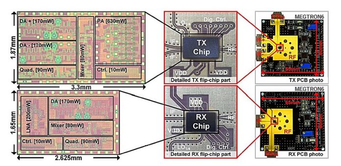
This innovative chipset covers a 56 GHz signal-chain bandwidth within the D-band (114–170 GHz). It includes a transmitter integrated circuit (IC) measuring 1.87 mm x 3.30 mm and a receiver IC measuring 1.65 mm x 2.60 mm. These components are designed to maintain signal speed and quality across a broad frequency range.
Key components of the chipset include power amplifiers to boost signal levels, low-noise amplifiers to enhance signal strength while reducing noise, mixers to adjust signals to the desired frequency range, distributed amplifiers for signal linearity, and frequency multipliers to quadruple the frequency.
To test the chipset’s wireless transmission capabilities, the researchers mounted it on a printed circuit board (PCB) and connected it to an external antenna with a gain of 25 dBi.
They converted the signal from a transmission line format, typically used on PCBs, to a waveguide format, which is used for high-frequency signal transmission in wireless applications. The conversion loss was kept to 4 dB.
This breakthrough development in wireless technology holds the potential to revolutionize the next generation of mobile communication systems, providing unprecedented speeds and reliability.


