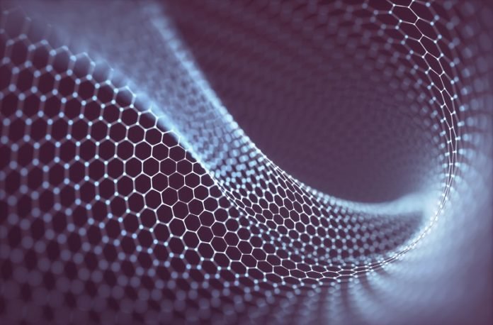
Researchers describe how electrons move through two-dimensional layered graphene, findings that could lead to advances in the design of future quantum computing platforms.
A new study published in Physical Review Letters describes how electrons move through two different configurations of bilayer graphene, the atomically-thin form of carbon.
Researchers could use to design more powerful and secure quantum computing platforms in the future.
“Today’s computer chips are based on our knowledge of how electrons move in semiconductors, specifically silicon,” says first and co-corresponding author Zhongwei Dai, a postdoc at Brookhaven.
“But the physical properties of silicon are reaching a physical limit in terms of how small transistors can be made and how many can fit on a chip.
If we can understand how electrons move at the small scale of a few nanometers in the reduced dimensions of 2-D materials, we may be able to unlock another way to utilize electrons for quantum information science.”
When a material is designed at these small scales, to the size of a few nanometers, it confines the electrons to a space with dimensions that are the same as its own wavelength, causing the material’s overall electronic and optical properties to change in a process called quantum confinement.
In this study, the researchers used graphene to study these confinement effects in both electrons and photons, or particles of light.
The work relied upon two advances developed independently at Penn and Brookhaven.
Researchers at Penn, including Zhaoli Gao, a former postdoc in the lab of Charlie Johnson who is now at The Chinese University of Hong Kong, used a unique gradient-alloy growth substrate to grow graphene with three different domain structures: single layer, Bernal stacked bilayer, and twisted bilayer.
The graphene material was then transferred onto a special substrate developed at Brookhaven that allowed the researchers to probe both electronic and optical resonances of the system.
“This is a very nice piece of collaborative work,” says Johnson. “It brings together exceptional capabilities from Brookhaven and Penn that allow us to make important measurements and discoveries that none of us could do on our own.”
The researchers were able to detect both electronic and optical interlayer resonances and found that, in these resonant states, electrons move back and forth at the 2D interface at the same frequency.
Their results also suggest that the distance between the two layers increases significantly in the twisted configuration, which influences how electrons move because of interlayer interactions. They also found that twisting one of the graphene layers by 30° also shifts the resonance to a lower energy.
“Devices made out of rotated graphene may have very interesting and unexpected properties because of the increased interlayer spacing in which electrons can move,” says co-corresponding author Jurek Sadowski from Brookhaven.
In the future, the researchers will fabricate new devices using twisted graphene while also building off the findings from this study to see how adding different materials to the layered graphene structure impacts downstream electronic and optical properties.
“We look forward to continuing to work with our Brookhaven colleagues at the forefront of applications of two-dimensional materials in quantum science,” Johnson says.
Written by Erica K. Brockmeier.


