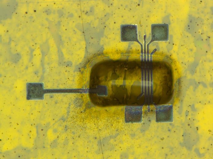
Engineers at Duke University have developed a groundbreaking method for printing fully functional and recyclable electronics at incredibly small, sub-micrometer scales—a major leap that could revolutionize how electronic displays are made and recycled.
The new process could not only reshape the $150 billion global display industry but also dramatically reduce its environmental footprint.
The research was published in Nature Electronics.
“If we want to seriously increase U.S.-based manufacturing in areas dominated by global competitors, we need transformational technologies,” said Aaron Franklin, the Edmund T. Pratt, Jr. Distinguished Professor of Electrical and Computer Engineering and Chemistry at Duke.
“Our process prints carbon-based transistors that can be fully recycled and perform comparably to industry standards. It’s too promising not to pursue further.”
From televisions and smartphones to car dashboards and smartwatches, digital displays are everywhere—and nearly all of them are made overseas, mainly in South Korea, China, and Taiwan.
Their production is energy-intensive, relying on vacuum-based processes that emit large amounts of greenhouse gases.
To make matters worse, only about one-quarter of the millions of tons of electronics discarded each year are recycled, according to United Nations estimates.
Franklin’s lab has been exploring ways to make electronics more sustainable. A few years ago, they developed the world’s first fully recyclable printed electronics, using a method called aerosol jet printing.
However, that approach could only create features larger than 10 micrometers—too big for use in modern consumer electronics, which require components hundreds of times smaller.
In the new study, Franklin and his team broke that size barrier by partnering with Hummink Technologies, a company specializing in precision printing.
Hummink’s “high-precision capillary printing” technology uses natural surface tension forces to pull extremely small droplets of ink through a tiny nozzle, similar to how paper towels draw in liquid.
This allows the printer to deposit precise, nanoscale patterns with remarkable control.
Using three carbon-based inks made from carbon nanotubes, graphene, and nanocellulose, the team successfully printed electronic components on both rigid surfaces like glass and flexible materials like paper.
These inks, refined from Franklin’s earlier work, were adjusted to flow perfectly with Hummink’s printers.
The result was the ability to print features only a few micrometers long, separated by gaps less than a micrometer wide—an essential requirement for making high-performance thin-film transistors (TFTs), the microscopic components that power every pixel in digital displays.
“These fabrication methods won’t replace silicon chips in computers,” Franklin said, “but they could be competitive—and even transformative—in the display industry.”
Every flat-panel display, from LCD to OLED, relies on millions of tiny transistors to control light and color.
In earlier research, Franklin’s team demonstrated that their printed transistors could drive LCD pixels, and he believes the new sub-micrometer versions are now close to powering OLED displays, which demand even higher performance.
Beyond displays, this technology could be used in sensors or flexible electronics. But for now, Franklin sees digital displays as the most promising path. The process consumes far less energy and emits fewer greenhouse gases than conventional manufacturing, while also enabling full recyclability—a major advantage for sustainability.
“Displays made with this kind of printing are the most realistic large-scale application I’ve ever seen come out of my lab,” said Franklin. “The biggest challenge now is securing the investment to take it to the next level.”
Despite recent funding setbacks, Franklin remains optimistic: “This technology has too much potential to ignore. It could be the key to a greener, more efficient future for electronics.”


