Photodetectors, the tiny devices that detect and measure light, are essential in technologies ranging from smartphones and wearable gadgets to autonomous vehicles and medical sensors.
But today’s photodetectors face a key limitation: they either require an external power supply or struggle with low sensitivity, particularly when made with traditional silicon semiconductors.
Now, researchers at the Korea Advanced Institute of Science and Technology (KAIST) have developed a self-powered photodetector that outperforms anything built before.
This device not only operates without electricity whenever light is present but also offers a sensitivity up to 20 times higher than existing detectors.
The breakthrough opens the door to ultra-precise, battery-free sensors for applications such as health monitoring, robotics, and next-generation electronics.
The research team, led by Professor Kayoung Lee from KAIST’s School of Electrical Engineering, achieved this milestone by solving a fundamental problem with two-dimensional semiconductors like molybdenum disulfide (MoS₂).
These materials are only a few atoms thick, which makes them ideal for creating ultra-small, highly responsive devices.
However, their thinness makes them difficult to “dope”—a process that involves adding impurities to adjust their electrical properties. Conventional doping can damage their delicate atomic structure, making it nearly impossible to build the kind of PN junction required for high-performance photodetectors.
A PN junction is the backbone of many light-sensitive devices, including solar cells. It is formed by joining two types of semiconductors: p-type, which has more positive charge carriers (holes), and n-type, which has more negative carriers (electrons).
When exposed to light, the junction allows current to flow in a controlled way, producing an electrical signal. Without doping, however, creating a reliable PN junction in 2D semiconductors seemed out of reach.
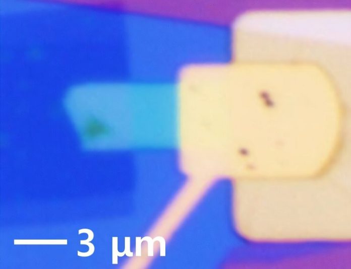
To overcome this challenge, Lee’s team designed a new device structure that eliminates the need for doping. They introduced a “partial gate” system, which applies an electrical signal only to part of the 2D material.
This clever design makes one side act like p-type and the other like n-type, effectively creating a PN junction without physically altering the semiconductor.
They also developed a “van der Waals bottom electrode,” which attaches to the semiconductor using gentle molecular forces rather than strong chemical bonds. This approach preserved the semiconductor’s delicate atomic structure while ensuring excellent electrical contact and signal transfer.
The result is a self-powered photodetector with a record-breaking responsivity of more than 21 amperes per watt—over 20 times higher than powered conventional sensors, 10 times higher than silicon-based self-powered sensors, and more than double the sensitivity of existing MoS₂ detectors.
Professor Lee explained that the achievement represents “a level of sensitivity unimaginable in silicon sensors” and emphasized its potential beyond just light detection. The same approach could be used to develop core components for smartphones, wearable electronics, and other devices that need to be smaller, more efficient, and capable of operating without external power.
By combining groundbreaking design with the unique properties of two-dimensional semiconductors, the KAIST team has set a new benchmark for photodetector performance—and taken a significant step toward the self-powered electronics of the future.


