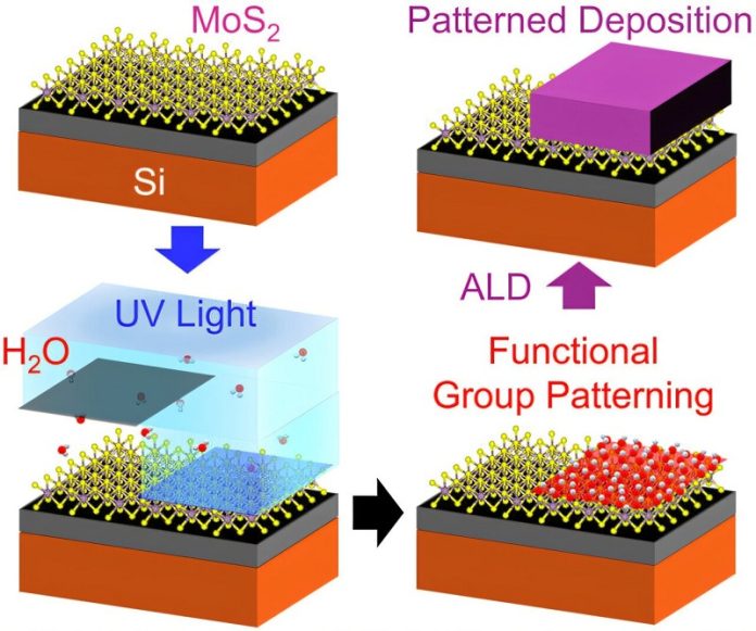
Scientists at the University of Missouri have developed a faster and cleaner way to manufacture computer chips using ultraviolet (UV) light.
This new technique could cut production steps in half, reduce harmful chemical use, and make chips more efficient.
Making computer chips is a complex process.
Today’s chips are packed with billions of tiny switches called transistors, which control the flow of electricity in everything from smartphones to laptops. To build them, engineers often use a method called atomic layer deposition, or ALD. This technique adds super-thin layers of material to the surface of a chip.
But there’s a problem—ALD spreads the coating over everything, including areas that aren’t supposed to be covered. It’s a bit like painting your whole house in one go and accidentally covering the windows too.
To fix this issue, the Mizzou research team created a more precise method called ultraviolet-enabled atomic layer deposition (UV-ALD).
This version of ALD uses UV light to “activate” only the areas that need to be coated. Once UV light hits a specific part of the chip, that spot becomes sticky, allowing the metal oxide material to attach only where it’s needed.
This targeted process reduces waste and avoids the problem of covering the wrong parts of the chip.
Matthias Young, the assistant professor leading the research, explained that this new process can cut down the traditional four or five steps required in chip manufacturing to just two. By simply shining UV light on the desired areas and applying the coating, the chip can be built much more efficiently.
Another big benefit of this new method is its environmental impact. Fewer manufacturing steps mean fewer harsh chemicals are needed. That’s not only safer for the people who work in chip factories but also better for the environment.
According to Andreas Werbrouck, a postdoctoral researcher and co-author of the study, this streamlined method could lead to safer working conditions and less chemical waste.
The team tested this method using a material called molybdenum disulfide (MoS₂), which is being studied as a promising component in the next generation of computer chips. Their results show that the UV-ALD method can successfully apply coatings to MoS₂ in a controlled and efficient way.
This research was conducted at the MU Materials Science and Engineering Institute, a joint effort between the College of Engineering and the College of Arts and Science at the University of Missouri.
Their findings were published in the journal Chemistry of Materials and could mark an important step forward in how we build the technology that powers our daily lives.


