A team of researchers from the University of Strathclyde has taken a major step forward in developing next-generation optical chips—tiny devices that control light for use in technologies like quantum computing, telecommunications, and advanced sensors.
The new method, published in Nature Communications, solves a long-standing problem in manufacturing miniature light-controlling structures called photonic crystal cavities, or PhCCs.
These structures are incredibly small—about the width of a human hair—but they can trap and guide light with extreme precision, making them essential for high-performance optical devices.
However, until now, making many identical PhCCs on a single chip has been nearly impossible. Even the smallest flaws during the manufacturing process—just billionths of a meter in size—can change how each PhCC behaves.
This means that most chips end up with mismatched components, limiting their use in practical, large-scale systems.
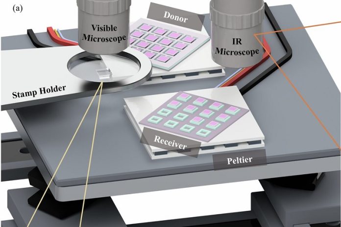
To overcome this, the Strathclyde researchers developed a new approach. Instead of trying to build perfect PhCCs directly on a chip, they first fabricate them separately and then move them one by one onto a new chip. As each PhCC is transferred, its optical properties are measured in real time to make sure it performs exactly as needed.
This is made possible by a custom-built integration system designed at Strathclyde, which allows for extremely accurate handling of these tiny structures.
According to Dr. Sean Bommer, the study’s lead author, previous attempts to build these chips were like putting together a Lego set without knowing the color or type of each brick. Now, the team can see exactly how each component behaves as they place it, allowing for much more reliable and advanced designs.
In one experiment, the team successfully transferred and sorted 119 PhCCs by their resonant wavelengths—the specific light wavelengths they interact with most strongly. Creating such a precise and ordered array would not be possible using traditional manufacturing methods.
The system also let the researchers observe, for the first time, how these microscopic devices change shape during the printing process. Some parts bent or stretched slightly, and the team could track how long it took them to return to normal, offering new insights into the mechanical behavior of these structures.
Professor Michael Strain, who leads the Chipscale Photonics group, says this breakthrough makes it possible to combine a wide variety of tiny semiconductor devices on one chip.
This opens the door to building much more powerful and flexible optical systems for everything from faster internet and smarter sensors to the future of quantum technologies.


