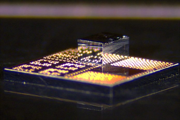
MIT researchers have developed a clever new way to make computer chips faster, more energy-efficient, and cheaper—by using just a tiny amount of a powerful material called gallium nitride (GaN).
While GaN has been known for decades and is used in things like LED lights and radar systems, it’s been too expensive and complicated to use widely in electronics like smartphones or computers. That might be about to change.
The new method developed by MIT and its partners allows tiny GaN transistors—tiny switches that control electrical signals—to be added directly on top of regular silicon chips, the kind used in most of today’s electronics.
These hybrid chips could lead to faster internet, clearer phone calls, better wireless signals, and longer battery life.
The innovation lies in how the GaN transistors are made and attached. First, researchers create thousands of tiny transistors on a GaN chip.
Then they cut each one out into small pieces just a few hundred microns in size (a micron is a millionth of a meter).
These mini-transistors, called “dielets,” are bonded onto a silicon chip using a low-heat process and copper instead of expensive gold. This method is much more affordable and avoids damaging the delicate materials.
What’s exciting is that this process only needs a tiny amount of GaN. That keeps costs low while still providing the high performance GaN is known for. Because the GaN transistors are so small and separated across the chip, they also help keep the whole system cooler, which is important for efficiency and performance.
In their demonstration, the researchers built a key part of wireless communication systems called a power amplifier. This component boosts signals in devices like smartphones.
Their amplifier was smaller than a square millimeter and outperformed traditional silicon-based versions.
It offered stronger signals, higher efficiency, and wider bandwidth—all things that help improve call quality, internet speed, and energy use in your phone.
The real breakthrough is that this process fits into the existing chip manufacturing system, meaning it could be added to current electronics and future ones without requiring brand-new factories. It’s also potentially useful for emerging fields like quantum computing, since GaN performs well at extremely cold temperatures required for those systems.
The research team even designed a special tool to precisely place the tiny GaN pieces onto the silicon chip, using vacuum suction and nanometer-level accuracy. The bonding is done with low heat and pressure, avoiding damage and keeping costs low.
This work opens the door to powerful, compact chips that blend the best of two worlds: the affordability and flexibility of silicon with the speed and strength of gallium nitride. Experts in the field believe it could play a key role in pushing technology forward, especially in the race to build faster, more energy-efficient wireless networks and computing systems.
As smartphones and digital devices continue to demand more power in smaller sizes, this new chip design may be just what the tech world needs to keep up.


