Researchers at Boise State University have developed a new way to make flexible electronic circuits that’s cheaper, faster, and better for the environment.
Their method uses a special material called laser-induced graphene (LIG) and was recently featured on the cover of Advanced Materials Technologies.
Laser-induced graphene is created by shining a laser onto carbon-rich materials, which turns them into a thin, conductive form of carbon known as graphene. This process forms a porous, three-dimensional structure that can carry electricity.
The best part?
It’s all done in a single step, without using harmful chemicals or creating excess waste.
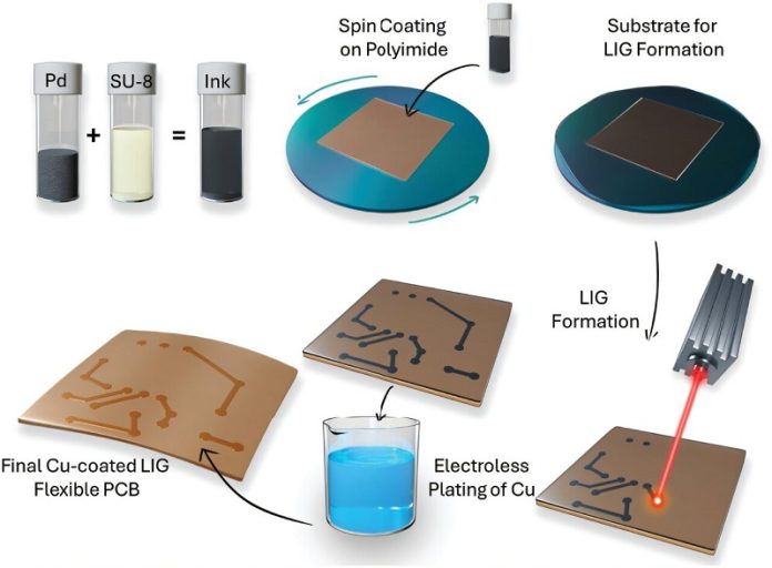
In their latest work, the Boise State team took this technology further by mixing palladium (a rare metal) nanoparticles into a soft plastic-like material.
When this mix is hit with a laser, it forms a special kind of LIG that has tiny palladium particles throughout.
These particles act like “seeds” that help grow a layer of copper using a chemical process called electroless deposition. The result is a network of copper wires built into a flexible circuit.
These copper connections—called interconnects—can be used with small electronic parts to build flexible hybrid devices. For example, the researchers created a flexible operational amplifier that can sense changes in resistance while being bent repeatedly.
This proves that the technology works for real-world electronics, even when those electronics need to flex and bend—something very useful for wearable devices.
According to lead author Attila Rektor, this method could revolutionize how we make printed circuit boards (PCBs). Traditional PCB manufacturing uses multiple steps, toxic chemicals, and a lot of material waste. This new technique uses less material, skips harmful etching steps, and can be done quickly—all while being more environmentally friendly.
Flexible PCBs are already in high demand because they save space, are lightweight, and can bend without breaking.
These qualities make them perfect for wearable health devices, fitness trackers, and smart clothing. As the global market for PCBs grows—expected to reach over $150 billion in the next decade—this green, cost-effective method could make a big impact.
Professor David Estrada, one of the study’s senior authors, says this breakthrough shows how science can go from the lab to real-life products.
“Attila’s work not only advances our understanding of materials but also shows a cleaner, smarter way to manufacture flexible electronics,” he said.


