Scientists in China have discovered a better way to build small, high-performance electronic parts using ultra-thin materials called 2D semiconductors.
These materials are only a few atoms thick and could be used to make faster, more efficient devices.
However, one big problem has been how to move these materials onto surfaces cleanly without damaging them or reducing their performance.
Researchers from Peking University, the Beijing Graphene Institute, and other institutions have now created a new method to solve this problem.
Their technique allows 2D semiconductors to be safely combined with special insulating materials called dielectrics, which help control electric charge in electronic devices.
Their method, published in Nature Electronics, involves growing a very thin layer of dielectric material on top of graphene—a well-known 2D material—using a process called epitaxial growth.
The graphene sits on a copper surface during this process. Later, the entire stack is transferred onto other surfaces with almost no damage.
In traditional methods, sticky polymers are used to help move these materials, but this often causes chemical contamination and physical damage.
That’s why this new method is so important—it keeps the graphene clean and its properties intact, while making the whole process more reliable.
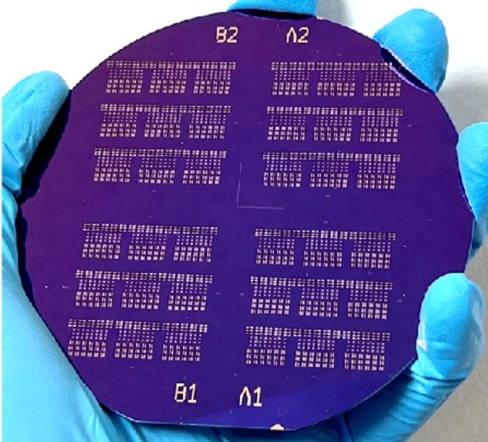
To prove that their idea works, the team used a dielectric called antimony oxide (Sb₂O₃). First, they grew a single-crystal layer of Sb₂O₃ on graphene that had been grown on a copper surface. Then, they treated the copper with a special water-ethanol solution, which made it easier to separate the layers.
This method allowed them to move a full 4-inch sheet of graphene onto another surface without damaging it. The electrical performance of the material remained excellent, with high carrier mobility—meaning the material allows electric charge to move quickly and efficiently.
The devices they made were also very stable over time, even when left in the open air.
This breakthrough could lead to new types of electronics and optical devices that are faster, smaller, and use less power. It may also help manufacturers build devices more easily on a large scale.
Next, the research team plans to take things further by stacking layers of 2D materials to create more complex 3D structures. These stacked devices could lead to even more powerful and compact electronics, but the team says this will require solving new challenges like making sure the layers connect properly and stay clean.
This research brings us one step closer to the future of electronics, where tiny, efficient, and powerful devices become part of our everyday lives.


