A new discovery in the world of tiny materials could lead to exciting advancements in electronics, such as super-efficient transistors or ultra-dense data storage.
A team led by Professor Catherine Dubourdieu, from HZB and FU Berlin, has developed nano-sized structures on silicon that can be electrically controlled, offering potential breakthroughs in future technology.
The research, published in Nature Communications, focuses on tiny islands made of a material called BaTiO3 (barium titanate).
These “nanoislands” are incredibly small, with dimensions of just 30–60 nanometers.
What makes them remarkable is their ability to form stable patterns of electric polarization—regions where electrical charges naturally align in a specific way.
The team created the nanoislands by carefully treating silicon wafers.
“By fine-tuning the first steps of silicon wafer preparation, we were able to form these nanoislands,” explained team member Dong-Jik Kim.
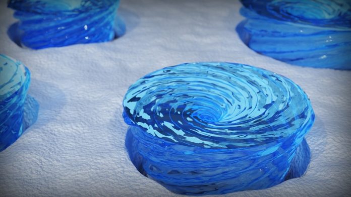
The resulting islands have a trapezoidal shape and a unique swirling electric texture, resembling tiny whirlpools. Using advanced tools like piezoresponse force microscopy (PFM) and scanning transmission electron microscopy (STEM), the researchers studied how the electric polarization behaves in these nanoislands.
One exciting finding is that these nanoislands exhibit a “vortex-like” texture, where electric charges seem to spiral inward, much like water swirling into a funnel. This swirling pattern is called chirality, and it’s rarely seen in nanoscale materials.
The team also discovered that these patterns can be reversed by applying an electric field. For example, the center-down polarization can be switched to center-up polarization. This reversibility makes these nanoislands highly promising for electronic applications.
Stabilizing and controlling such swirling patterns, known as chiral topological textures, has been a major challenge for scientists. Dubourdieu explains: “In this work, we’ve shown that by shaping nanostructures in the right way, we can stabilize these textures.”
This ability to manipulate swirling, polar patterns in BaTiO3 opens up possibilities for new kinds of electronic devices. For instance, the technology could lead to extremely efficient field-effect transistors or devices capable of storing enormous amounts of data in a very small space.
The discovery of these controllable swirling textures is a big step forward in nanoelectronics. By continuing to explore how these patterns can be used, scientists hope to develop innovative devices for computing, memory storage, and beyond.
“These chiral topological textures are not only fascinating but also incredibly promising for future applications,” Dubourdieu said. The findings could shape the future of tiny, powerful electronics.


