Nanoelectronics power our everyday lives, from smartphones and computers to medical devices.
This field focuses on creating tiny components, like transistors and circuits, that fit on the tip of a needle.
To make these devices more energy-efficient and powerful, scientists are exploring alternatives to traditional silicon-based semiconductors.
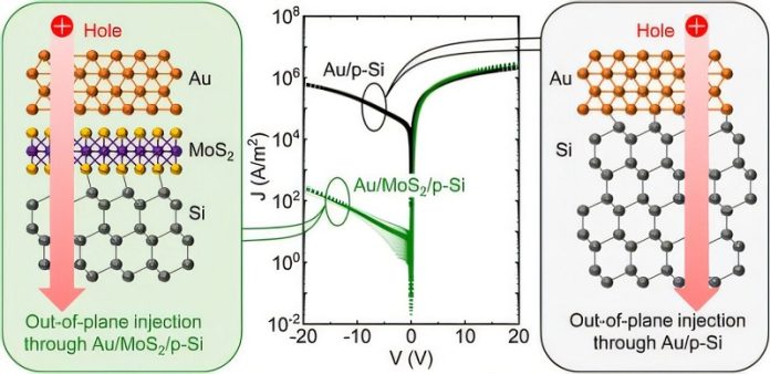
A recent study, led by the University at Buffalo and published in ACS Nano, shows how combining silicon with ultra-thin, two-dimensional (2D) materials could revolutionize semiconductor technology.
This breakthrough offers a better way to inject and transport electric charges, paving the way for more efficient and compact devices.
Dr. Huamin Li, the study’s lead author and associate professor in electrical engineering, explains the goal: “Our work investigates how emerging 2D materials can enhance existing silicon technology, boosting performance and energy efficiency in nanoelectronics.”
The research team, which includes experts from the U.S., China, Korea, Austria, and Italy, demonstrated that combining silicon with a 2D material like molybdenum disulfide (MoS2) results in highly efficient electronic devices.
Despite being less than one nanometer thick, the 2D material acts as a bridge, controlling how electrical charges are injected and transported in the device.
Interestingly, the study revealed that while the 2D material impacts how charges enter the system, it has little effect on how they exit.
“Whether you use MoS2, graphene, or another 2D material, they behave similarly when collecting charges,” said Li. “In this special condition, the 2D layer acts almost like it’s invisible or has no resistance for charge collection.”
Dr. Fei Yao, co-lead author and assistant professor in materials design, highlighted the importance of miniaturization. “Making components smaller allows us to create advanced, compact technology,” she said. The team’s findings could lead to more powerful, space-saving electronics in the future.
The research also provides valuable insights into how charges move at the boundary where 2D and 3D materials meet. Understanding these mechanisms is crucial for developing next-generation devices.
While integrating 2D materials with silicon holds great promise, challenges remain. Scientists must further explore and refine how these materials work together. “Our study lays the groundwork for developing new materials and device concepts,” Li said. “This could ultimately lead to more efficient electronics for everyday use.”
This collaborative research showcases the University at Buffalo’s leadership in advanced semiconductor technologies. By combining international expertise, it’s paving the way for a greener, smarter, and more energy-efficient tech future.


