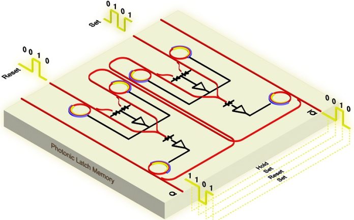
Researchers have developed a groundbreaking optical memory device called a programmable photonic latch, promising faster and more efficient data storage for optical systems.
This new technology, designed using silicon photonics, is a significant step forward in optical data processing and could pave the way for next-generation computing.
The photonic latch works like a simple memory unit in electronic devices, switching between “set” (1) and “reset” (0) states to store a single bit of information.
While optical computing and communications have made great progress in recent years, data storage has mostly relied on slower electronic memory.
This breakthrough offers a fast and scalable alternative for temporary storage in optical systems, reducing energy use and speeding up data processing.
Farshid Ashtiani from Nokia Bell Labs, the lead researcher, explained the potential impact: “Fast optical memory integrated with optical systems could improve efficiency and throughput in communications, computing, and sensing technologies.”
In their study, published in Optics Express, the team demonstrated the photonic latch on a programmable silicon photonic platform.
This system offers features like optical set and reset, complementary outputs, and compatibility with wavelength division multiplexing (WDM). These qualities make the memory highly scalable and suitable for use in advanced optical systems.
Ashtiani highlighted its relevance for technologies like AI, saying, “Large language models such as ChatGPT rely on rapid calculations to process and generate responses.
Our optical memory could significantly boost the speed of such operations. While commercial optical computers are still in the future, this is a step toward making them possible.”
Traditional optical memory systems are often large, expensive, and energy-hungry, requiring specialized materials.
The new photonic latch overcomes these issues by using silicon photonic micro-ring modulators, which are compatible with commercial chip manufacturing.
These modulators form the basis of universal logic gates, combined to create the photonic latch.
The system’s scalability is a key advantage. Each memory unit operates independently, without interference from others, allowing for reliable, high-yield production.
Additionally, the memory’s ability to work with WDM enables multi-bit storage within a single unit, making it highly efficient. The response time, measured in tens of picoseconds, far exceeds the speeds of most digital systems.
To prove their concept, the researchers tested the device using simulations and experiments. The photonic latch reliably performed functions like setting, resetting, and holding data, even when input power varied.
Next, the team aims to scale the technology, create dedicated photonic memory chips, and integrate photonic circuits with electronics in a single manufacturing process. This would allow for even greater memory density and pave the way for faster, more efficient optical computing systems.


