Imagine being able to adjust the surface of a material with atomic-scale precision using just a laser.
What sounds like science fiction has now become reality, thanks to groundbreaking research published in Applied Surface Science.
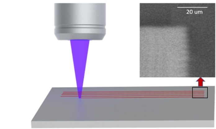
A team of scientists, led by Dr. Mojtaba Moshkani, has developed a laser technique that allows for the precise manipulation of diamond surfaces in ordinary air, without the need for complex vacuum equipment.
“Our method provides atomic-level control over diamond surfaces in a standard air environment,” says Dr. Moshkani. “This is truly remarkable for such a simple process.”
The technique uses a deep ultraviolet (UV) laser to carefully remove tiny amounts of material—down to just 1 percent of a single atomic layer.
By delivering short pulses of laser light, the researchers trigger localized chemical reactions on the diamond surface.
These reactions selectively remove carbon atoms from the topmost atomic layer, giving researchers unprecedented control over the diamond’s structure and properties.
This innovation has huge implications for electronics, quantum technologies, and advanced manufacturing.
Even small changes to the arrangement of surface atoms can drastically improve a material’s performance.
One of the study’s most exciting discoveries was a significant boost in the electrical conductivity of treated diamond surfaces—up to seven times higher than untreated surfaces. This result was confirmed by collaborators at MIT Lincoln Laboratory.
“We were amazed that such a minor adjustment could yield such a dramatic improvement in conductivity,” says team leader Professor Richard Mildren.
This breakthrough could help make diamonds a more viable material for semiconductors.
Diamonds are already valued for their high thermal conductivity and resistance to electrical breakdown, making them ideal for high-power and high-frequency electronic devices.
The new laser method is not only precise but also incredibly fast. In current experiments, the laser removed 1 percent of a monolayer in just 0.2 milliseconds. This speed makes the process suitable for large-scale industrial applications, such as wafer processing.
Dr. Moshkani adds, “The process is rapid and scalable, making it a strong option for industries that require advanced material processing.”
Beyond electronics, this technique could play a vital role in advancing quantum technologies. Diamond surfaces are critical for stabilizing quantum states, such as those used in quantum computers. The ability to engineer diamond surfaces with atomic precision could revolutionize the field.
“This is just the beginning,” says Professor Mildren. “We’re excited to explore how this technique can unlock the full potential of diamonds in electronics, quantum technologies, and beyond.”
This breakthrough marks a significant step forward in material science, with the potential to transform industries and pave the way for exciting new applications.


