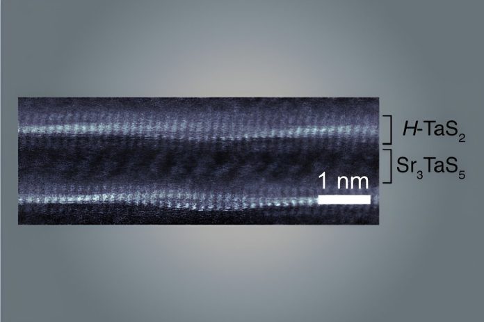
MIT physicists, along with their colleagues, have developed a new material with unique superconducting and metallic properties, thanks to its wavy layers of atoms.
These layers are incredibly thin, just billionths of a meter thick, and they repeat over and over to create a sample that’s large enough to hold in your hand.
The ability to make a sizable sample of this material makes it easier for scientists to explore how it behaves at the quantum level, where the strange properties of atoms come into play.
This work, published in the journal Nature, is especially significant because the material was created through “rational design.”
This means the researchers used their understanding of materials science and chemistry to carefully plan and create the material. Because of this approach, the scientists are confident that they can design and create even more new materials with unusual and exciting properties.
While there are other materials with wavy atomic structures, the MIT team believes theirs is the most perfect. The waves in the atomic layers are consistent across the entire crystal, which is made up of thousands of these corrugated layers.
“Materials like this go beyond what we typically think of as a crystal,” says Joseph Checkelsky, the senior researcher and Associate Professor of Physics at MIT. “Understanding what new physical properties might emerge from this is an exciting opportunity.”
The promise of 2D materials
Two-dimensional (2D) materials, which consist of just one or a few layers of atoms, have caught the attention of physicists because they can be manipulated to show new and unusual properties.
For example, if you slightly twist one layer of atoms in a 2D material relative to another layer, it can create a special pattern called a moiré superlattice.
This pattern can lead to phenomena like superconductivity (where electricity flows without resistance) and unconventional magnetism.
However, moiré materials are difficult to make because they need to be assembled by hand, layer by layer. They’re also hard to study because of their tiny size. Checkelsky’s team has been working on creating similar materials that are much easier to handle and investigate.
How the Material Was Made
The process of creating this new wavy material is relatively straightforward.
“We basically mix powders of the necessary materials, heat them to a few hundred degrees Celsius in a furnace, and let chemical reactions naturally form large crystals with properties controlled by atomic-scale interactions,” says Aravind Devarakonda, a former MIT Ph.D. student and now an assistant professor at Columbia University. Devarakonda is the lead author of the Nature paper.
In 2020, Checkelsky and many of the same colleagues reported creating the first such material in a paper published in Science.
Then, in 2021, they explained in Nature how that material could exhibit two different kinds of superconductivity. The new wavy material is the second member of this growing family of compounds.
Like a Layer Cake
The new material resembles a layer cake. It’s made of atom-thin layers of tantalum and sulfur, which are stacked on top of a “spacer” layer made of strontium, tantalum, and sulfur.
This pattern repeats thousands of times to create a large crystal.
The waves in the material likely form because there’s a mismatch in the size and structure of each layer’s crystal lattice. This causes one layer to buckle, like paper folding upwards, to fit on top of another layer. The result is a series of minuscule waves.
Interesting Properties
These tiny waves are what give the material its interesting properties. For instance, at certain temperatures, the material can become superconducting, allowing electrons to flow without any resistance.
However, the superconductivity in this material is not uniform—it’s influenced by the waves. In some areas, it’s stronger, while in others, it’s weaker.
The material also has unusual metallic properties because electrons find it easier to move through the valleys of the waves rather than over the peaks.
Devarakonda explains, “We’ve shown that by introducing the wave structure, we can drastically change the behavior of the layers.
We’ve opened up an entirely new family of materials, and the possibilities are endless. It’s exciting to see what surprises the future holds.”


