A team of researchers, led by Director Jo Moon-Ho of the Center for Van der Waals Quantum Solids at the Institute for Basic Science (IBS), has discovered a new way to grow ultra-small transistors.
They used a novel technique to create 1D metallic materials that are less than 1 nanometer wide.
This breakthrough could lead to the development of incredibly small and efficient semiconductor logic circuits.
Their research was published in Nature Nanotechnology.
Two-dimensional (2D) semiconductors, which are only a few atoms thick, have become a major focus for researchers due to their excellent properties.
However, making ultra-miniaturized transistors that can control electron movement within just a few nanometers has been extremely challenging.
In transistors, the gate electrode controls the flow of electrons. The ability to make this gate very small is crucial for creating more integrated and powerful semiconductor devices.
Traditional methods struggle to make gate lengths smaller than a few nanometers because of limitations in lithography, a key process in semiconductor manufacturing.
To overcome this, the research team used a special feature of molybdenum disulfide (MoS2), a 2D semiconductor.
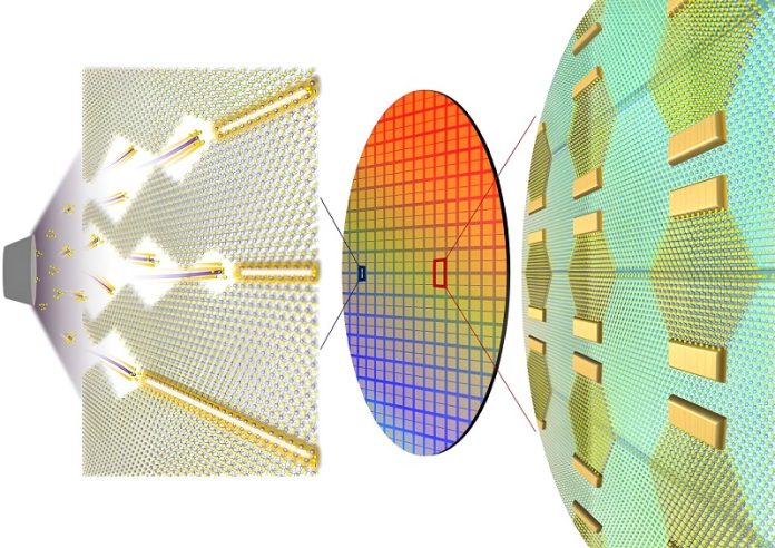
They discovered that a part of MoS2 called the mirror twin boundary (MTB) acts as a 1D metal with a width of only 0.4 nanometers. By using this 1D metal as a gate electrode, they bypassed the limitations of lithography.
This image shows an optical microscope view of an integrated circuit based on 1D MTB gates (left), a diagram of the ultra-miniaturized transistor and inverter devices in the circuit (center), and the performance of these devices (right).
The research team successfully used their 1D MTB process not only to miniaturize individual devices but also to create large-area, highly integrated electronic circuits.
In their study, the team achieved the 1D MTB metallic phase by precisely controlling the crystal structure of the 2D semiconductor, turning it into a 1D metal. This represents a significant advancement for both next-generation semiconductor technology and basic materials science, as it shows how new material phases can be created over large areas through controlled crystal structures.
According to the IEEE’s International Roadmap for Devices and Systems (IRDS), semiconductor technology is expected to reach around 0.5 nanometers by 2037, with transistor gate lengths of 12 nanometers. The research team demonstrated that their 1D MTB gate can control channel widths as small as 3.9 nanometers, far surpassing these predictions.
The 1D MTB-based transistor also offers better circuit performance. Current technologies like FinFET or Gate-All-Around, used to miniaturize silicon semiconductors, often suffer from parasitic capacitance, which can destabilize highly integrated circuits. In contrast, the simple structure and extremely narrow gate width of the 1D MTB-based transistor minimize these issues.
Director Jo Moon-Ho stated, “The 1D metallic phase achieved through epitaxial growth is a new material process that can be applied to ultra-miniaturized semiconductor processes. It is expected to become a key technology for developing various low-power, high-performance electronic devices in the future.”


