MIT engineers have created a new computer vision technique that significantly speeds up the process of analyzing new electronic materials.
This method is 85 times faster than traditional approaches and could help improve solar cells, transistors, LEDs, and batteries by quickly identifying promising new materials.
The search for better electronic materials is crucial for improving the performance of various devices.
Scientists use AI to sift through millions of chemical formulations to find potential materials.
Engineers then use machines to print hundreds of material samples at once, based on AI suggestions. However, confirming that these materials work as expected has been slow, creating a bottleneck in the process.
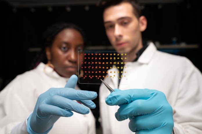
The new technique developed at MIT uses computer vision to analyze images of printed semiconductor samples. It quickly estimates two key properties of each sample: the band gap (which measures electron activation energy) and stability (which measures longevity).
This technique can characterize materials much faster than the conventional method, which involves a domain expert manually examining each sample.
Eunice Aissi, an MIT graduate student, explains, “We envision fitting this technique into an autonomous lab of the future.
The system would allow us to give a computer a materials problem, have it predict potential compounds, and then run 24-7 making and characterizing those predicted materials until it finds the best solution.”
Traditional material characterization is done using a tool called UV-Vis, which scans through different colors of light to determine where a semiconductor starts to absorb more strongly.
This method is precise but slow, with an expert characterizing about 20 samples per hour. Some printing tools, however, can produce 10,000 material combinations per hour, creating a mismatch in the process.
To solve this, the MIT team turned to computer vision, a field that uses algorithms to analyze images quickly. “Optical characterization methods are powerful,” says professor Tonio Buonassisi. “You can get a lot of information quickly that a human can’t process but a computer can.”
The researchers developed two algorithms: one to estimate the band gap from hyperspectral images (which have 300 channels of color information) and another to assess stability from standard RGB images.
The team tested their new technique on 70 printed semiconducting samples made from different ratios of perovskites, a promising but unstable material for solar cells. Using a hyperspectral camera, they scanned the samples and applied their band gap algorithm, completing the analysis in just six minutes.
For stability testing, the samples were placed in a chamber with varying environmental conditions. An RGB camera took images every 30 seconds for two hours, and the stability algorithm analyzed the color changes to estimate degradation.
The new method was compared with manual measurements by an expert. The results were 98.5% accurate for band gap and 96.9% accurate for stability, matching the expert’s estimates but 85 times faster.
“We were constantly surprised by how these algorithms could not only speed up the process but also provide accurate results,” says MIT graduate student Alexander Siemenn. “We plan to integrate this technique into a fully automated materials pipeline in our lab.”
This new method promises to revolutionize the way electronic materials are discovered and tested, potentially leading to faster advancements in various technologies. The research was supported in part by First Solar.


