In the vast and intricate world of materials science, understanding how to manipulate materials for our benefit is a bit like trying to navigate without a map.
Especially when we delve into the micro and nano scales, the behaviors of materials can surprise us.
One such surprise is the concept of elastic strain engineering, a technique that has now been mapped out for the first time by researchers at MIT, making it much clearer how we can tailor materials to enhance their properties for our technological advancements.
Imagine pulling or compressing a material and it snapping back to its original shape, like a rubber band.
This is what happens at a microscopic level with some materials when they undergo what’s called elastic strain.
For years, scientists knew that applying a bit of this strain could make materials perform better, but knowing exactly how to do this for the best results was a mystery—until now.
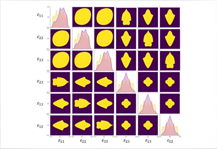
The team at MIT, led by Professor Ju Li, has taken a groundbreaking step by combining calculations and machine learning to produce a detailed map.
This map guides us on how to adjust strains on crystalline materials (imagine the structured patterns you see on snowflakes under a microscope) to achieve desired thermal and electronic properties.
It’s a bit like having a GPS for navigating the potential improvements in materials.
Previously, to enhance a material’s features, scientists mainly changed its chemical makeup.
However, Li’s team showed that by tweaking the strain in different directions—a technique offering six degrees of freedom—you could significantly alter a material’s behavior without altering its chemical composition.
This opens up a whole new avenue for material design, akin to having a multi-tool instead of a single screwdriver.
The foundations of this discovery were laid decades ago when it was found that semiconductor materials, used in electronics, doubled their performance with just a 1% application of strain.
This finding was quickly adopted by the semiconductor industry to boost microchip performance in electronic devices.
Yet, recent advancements have shown that materials like diamond can withstand much higher strains (up to 9%) and significantly alter their properties, such as transforming diamond, known for its insulating properties, into a potential semiconductor or even a conductor.
The MIT team’s map allows for an unprecedented level of precision in adjusting a material’s properties, offering the potential to create materials that conduct heat better or worse by significant factors.
This could lead to the development of computer chips that run faster and cooler, quantum sensors, and communication devices, by efficiently managing heat in denser electronic architectures.
Although the immediate application of these findings to everyday technology like laptops or cellphones might still require overcoming manufacturing challenges, the groundwork laid by this research offers an exciting glimpse into the future.
It signals a new era where material properties can be dialed in with precision, paving the way for technological innovations we’ve yet to imagine.
Source: MIT.


