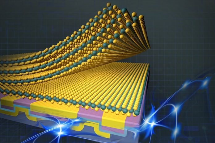
In the realm of modern technology, a team of researchers from MIT and other institutions have made a groundbreaking advancement in the use of two-dimensional (2D) materials for electronic devices.
These materials, incredibly thin and only a few atoms thick, have shown remarkable properties, like efficiently conducting electric charge.
This could significantly enhance the performance of future electronic devices.
However, incorporating these 2D materials into devices like computer chips has been a major challenge.
Their ultra-thin nature makes them susceptible to damage from traditional manufacturing processes that often involve harsh chemicals, high temperatures, or abrasive techniques like etching.
To address this problem, the researchers developed a novel technique that allows for the integration of 2D materials into devices in a way that preserves their pristine quality and maximizes their unique optical and electrical properties.
This method involves engineering surface forces at the nanoscale, enabling the 2D materials to be physically stacked onto other layers of a device without damage.
The team successfully used this approach to create arrays of 2D transistors with new functionalities, surpassing those made with conventional methods. This versatile technique has potential applications in high-performance computing, sensing, and flexible electronics.
At the core of this innovation is the formation of clean interfaces using van der Waals forces, natural forces of attraction that exist between all matter. These forces are critical in holding the materials together.
However, integrating materials into fully functional devices using van der Waals forces alone can be challenging, as some materials cannot be directly integrated due to the intrinsic properties of the materials involved.
The research, which will be published in Nature Electronics, tackles this limitation by developing a platform that enhances the versatility of van der Waals integration, paving the way for new device functionalities.
Traditional methods for creating complex systems like computer chips can be messy, often damaging the materials involved.
Recently, researchers have been focusing on building devices from the bottom up using 2D materials. This process involves physical stacking rather than using chemicals or high temperatures for bonding.
Though all materials exhibit van der Waals interaction, the strength of these forces varies, and they are not always sufficient to hold different materials together.
For example, a popular semiconducting 2D material, molybdenum disulfide, will adhere to metal like gold but won’t transfer directly to insulators like silicon dioxide just by physical contact.
Previously, integrating semiconductor and insulating layers, essential for electronic devices, required bonding the 2D material to an intermediate layer like gold, then transferring it to the insulator, followed by removing the intermediate layer using chemicals or heat.
The MIT team’s approach eliminates the need for this sacrificial layer. Instead, they embed the low-adhesion insulator in a high-adhesion matrix, which makes the 2D material stick to the embedded surface, thus creating a van der Waals interface between the 2D material and the insulator.
To construct electronic devices, they form a hybrid surface of metals and insulators on a carrier substrate, then flip it over to reveal a smooth top surface containing the device building blocks.
This smoothness is crucial for maintaining effective van der Waals interactions. The 2D material is prepared separately in a clean environment and then brought into direct contact with the device stack.
Once contact is made, the hybrid surface picks up the 2D layer, integrating it seamlessly. This process maintains the integrity of the 2D material interface, allowing it to achieve its maximum performance potential without being hindered by defects or contamination.
The researchers have demonstrated the ability to engineer the surface of the 2D material, creating features or connections to other components.
They have successfully created p-type transistors, which are typically difficult to make with 2D materials, and have shown improved performance compared to previous studies.
This method can be scaled up to make larger arrays of devices and is adaptable with various materials. For example, they integrated graphene onto a device using a polymer matrix, relying on chemical interactions in addition to van der Waals forces.
Looking ahead, the researchers aim to expand this platform to integrate a diverse array of 2D materials. This will enable the study of their intrinsic properties without the influence of processing damage and the development of new devices that leverage their superior functionalities.
This breakthrough marks a significant step forward in the field of electronics, offering a path to more efficient, high-performance devices.


