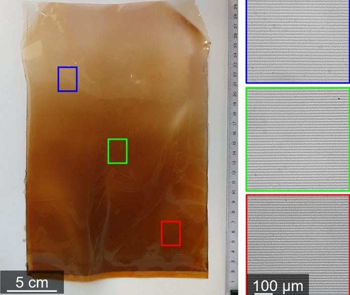
In the world of material science, a researcher named Christiaan Van Campenhout has stumbled upon a simple and low-cost way to create a high-tech material.
This material is made up of crystals arranged in regular bands or stripes, and the width and spacing of these bands can be controlled precisely.
The new method could make it much easier and cheaper to create things like electronics, optics, and sensors.
Van Campenhout and his team at AMOLF, who work in a group that explores how matter organizes itself, made a fascinating discovery that was recently shared in a scientific journal called Advanced Materials.
They started with a plain-looking brown plastic sheet, but when a laser beam was shone through it, a pattern of dots appeared on the other side.
This was because the plastic sheet had narrow bands of crystals inside it, arranged neatly in rows.
These bands of crystals were too small to see with the naked eye, but they had a huge impact on the laser light passing through the plastic.
Usually, creating such precise patterns requires high-tech, expensive methods like lithography. But Van Campenhout and his team are inspired by nature’s way of creating patterns, such as the stripes on a zebra or the spots on a butterfly’s wings.
They aim to find simple, nature-inspired methods to create high-tech materials, and this discovery is a big step forward in that direction.
The bands of crystals were formed by a chemical reaction that happens when a substance in a gel reacts with a substance in a liquid solution. The gel then turns into the plastic sheet, with the crystals embedded inside.
In earlier experiments, the researchers could create the crystal bands by slightly shrinking the gel. But this time, they tried something new. They slowly dipped the gel into the liquid, and this created the same pattern of bands.
Van Campenhout and his team named this process “R-DIP,” which stands for “reaction-diffusion driven immersion-controlled patterning.”
They found that the distance between the bands could be controlled by the speed at which the gel was dipped into the liquid. Faster dipping resulted in bands that were closer together.
Their aim is to get the bands even closer, down to a distance of 0.2 micrometers or less, for specific applications.
They also found that the method works with a larger sheet of plastic, which could be useful for manufacturing electronics on a large scale.
One possible application of the new material is in creating polarizing films for items like sunglasses and lenses. This would involve layering several sheets with bands on top of each other, each one slightly rotated.
Another application could be an ultra-sensitive pressure sensor. When two layers of the material are placed parallel to each other, they create a pattern that changes when they’re pressed together, even by a tiny amount.
In the future, Van Campenhout plans to explore if he can change the composition of the bands to make them more suitable for different applications, which could further expand the potential uses of this exciting new material.
He’s also interested in investigating whether the chemical knowledge from photography could be applied to develop films for other applications, given the similarities between the new material and photographic film.
Follow us on Twitter for more articles about this topic.
Source: AMOLF.


