Picture a pencil and how you can draw with it.
Now imagine that you can take a layer of graphite, the stuff that makes the mark, and make it as thin as a single atom.
Cool, right?
That’s what scientists call 2D material, and it’s not just about graphite or “graphene.”
There are many types of these extremely thin materials that could be used in advanced technology due to their unique properties.
But creating working devices with these 2D materials has been tricky because they’re incredibly delicate.
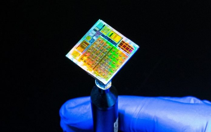
Fast forward to now, and a team of researchers at KAUST has made an exciting breakthrough – the world’s first fully working microchip made with 2D materials.
They were inspired by previous work done in their lab with these thin films.
How did they manage to pull this off?
Lanza, the lead researcher, explained that their goal was to improve the usefulness of 2D material-based electronic devices by using the standard technology found in our everyday electronic gadgets, such as smartphones.
The main problem they faced was that these ultra-thin materials can have tiny imperfections that might cause a device to fail. Also, integrating the 2D material into a microchip without damaging it was a big challenge.
To overcome these issues, the team carefully designed the chip to make it easy to build and reduce the impact of any defects. They fabricated normal electronic components on one side of the chip, made connections to the underside, and then transferred the 2D material there.
The 2D material they used was hexagonal boron nitride, or h-BN. They first created it on a piece of copper foil and then moved it onto the microchip using a low-temperature wet process. They were then able to form electrodes on top using standard techniques.
What’s so special about h-BN? Well, when it’s as thin as just 18 atoms (that’s super tiny, 6 nanometers!), it becomes a perfect “memristor.” Memristors are elements in a circuit whose resistance can be changed by voltage.
This lets them “remember” their state even after power is turned off. With their chip design, each memristor is connected to a single transistor, allowing precise control and high reliability. Essentially, this tiny chip can serve as a low-power brain cell in a neural network.
Lanza is excited about their achievement and is now in talks with top semiconductor companies to push this technology further.
They’re also planning on setting up their own system for producing 2D materials at a large scale at KAUST.
This breakthrough might just revolutionize the world of electronics!
Source: KAUST.


