As computers and electronic devices get smaller and smaller, engineers are developing new technologies to enable devices to shrink even further while improving performance.
One promising new technology is spintronics, which has the potential to make smaller and faster devices that retain their information when the power is off.
This emerging technology could revolutionize the design of electronic devices, but it still has a long way to go before the technology becomes mainstream.
To keep up with increasing data generation, data storage capacity has increased while electronic devices continue to get smaller and more powerful.
However, this increase in data generation and storage has led to an associated increase in energy consumption.
Data centers use a significant amount of electricity for their servers and cooling systems, and those centers alone account for more than 1% of global energy use.
Spintronics has the potential to cut this energy consumption while allowing engineers to continue to design smaller and faster computers and other electronic devices.
“The ability to manipulate the arrangement of electronic spins, as well as their movement through material, has tremendous possibilities for more energy-efficient devices.
This is the first step in demonstrating how to do it.” — Chang-Beom Eom, professor of materials science and engineering, University of Wisconsin-Madison
Instead of using electron charge to store information as 1’s and 0’s, spintronics uses electron spin to encode data. Spin is a property of electrons, just like charge.
Electrons can have a spin state that is either up or down, and in some special materials this spin state can move across the material when it’s exposed to electricity. The ability for the spin state to be transported is what allows spin to be used for data storage.
This method of spin manipulation for data storage uses much less energy because a spin current encounters less of the resistance that can lead to overheating, and the information does not disappear with a loss of power.
Researchers using the Advanced Photon Source (APS), a U.S. Department of Energy Office of Science User Facility at DOE’s Argonne National Laboratory, have been studying ways to manipulate electron spins and developing new materials for spintronics.
Recently, a research team led by Chang-Beom Eom, a professor of materials science and engineering at the University of Wisconsin-Madison, published a study in the journal Nature Communications about a new material that has three times the storage density and uses much less power than other spintronics devices.
Not many of these types of materials exist, especially ones that work at room temperature like this one.
If Eom’s material can be perfected, it could aid in the creation of more efficient electronic devices with less tendency to overheat.
This is particularly important to advancing the development of low-power computing and fast magnetic memory.
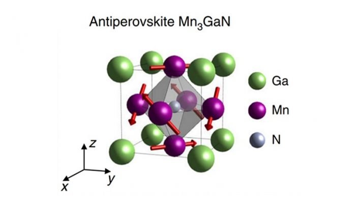
The new structure Eom designed is based on an unusual class of materials called antiperovskites that he uses to manipulate the flow of spin information without moving the electrons’ charges through the material.
To figure out if it worked, and to better understand the structure of the material, Eom’s team used X-ray diffraction at the APS to see at what point the structure of the material changed, indicating the emergence of the necessary arrangement of electronic spins.
Eom came to the APS because of the power of the 6-ID-B beamline as well as for the expertise of the scientists that work there.
“In one week of time at the APS we can do a month’s worth of work,” he said.
The APS’s beamline scientists provide expert advice to researchers looking to use the resources of the facility. Before the study, APS beamline scientists Phil Ryan and Jong-Woo Kim spent time with Eom, helping him determine when he had the right structure as he grew these new materials in his lab.
“If they have a scientific question, we discuss it and together design an experiment at APS to answer the question,” said Kim, a physicist at APS collaborating with Eom’s research team. “We understand our techniques and capabilities very well, so we can contribute to the design of the experiment, or even shape the conversation.”
For this study, Eom used the APS to look at the lattice structure of the material at the atomic level as it cooled toward room temperature.
Using X-ray diffraction, they measured the lattice parameter — basically the distance between atoms — and extracted the separation of the atoms as the temperature of the material changed.
“This material develops a magnetic order a little above room temperature,” said Ryan, another physicist at APS who worked with Eom on this project as well as many others over the years.
“Once the electron spins order themselves, the atoms are pushed slightly away from each other. So even though we couldn’t directly detect the structure with X-rays, we monitored and measured this structural change with temperature at the APS to confirm the emergence of this magnetic order.”
This was one of the three techniques used in the study to measure the arrangement of electronic spins, and this data, in conjunction with other measurements, helped solidify and cement the validity of the findings.
“The ability to manipulate the arrangement of electronic spins, as well as their movement through material, has tremendous possibilities for more energy-efficient devices,” Eom said. “This is the first step in demonstrating how to do it.”


