Silicon has long been the conventional material of choice for solar cells, which convert energy from the sun into electricity.
However, because light absorption in silicon is inefficient, solar cells made of silicon are thick, heavy, and rigid.
Moreover, their manufacturing is complex and expensive.
To address these issues, scientists have been trying to find alternatives to silicon.
Less than a decade ago, scientists began looking into organic-inorganic hybrid materials with a particular kind of crystal structure known as perovskite.
One of the most widely studied hybrid perovskites contains iodine and lead as the inorganic components and a compound consisting of carbon, hydrogen, and nitrogen (methylammonium) as the organic component.
Within the past few years, the efficiency of these perovskite-structured hybrid compounds has skyrocketed up to about 25 percent, surpassing that of some silicon solar cells.
Besides their efficiency, hybrid perovskite solar cells are attractive because they can be manufactured through simple, low-cost techniques such as spray coating.
But hybrid perovskite materials are not yet viable replacements to silicon, largely because of stability issues. Their performance quickly degrades when they are continuously exposed to moisture, light, and heat—all elements that a solar cell would experience in the natural environment.
Now, an international team led by professors Heejoo Kim and Kwanghee Lee of the Gwangju Institute of Science and Technology (GIST) in South Korea has developed new material processing steps that significantly improve the operational stability of hybrid perovskite solar cells.
Their processing method is described in a recent paper published online in Energy & Environmental Science.
Typically, thin-film devices are made in solution by sandwiching the active light-absorbing material in between top and bottom metal electrical contacts (electrodes) and organic semiconductor interlayers, which enhance the extraction of electrical currents to the contacts.
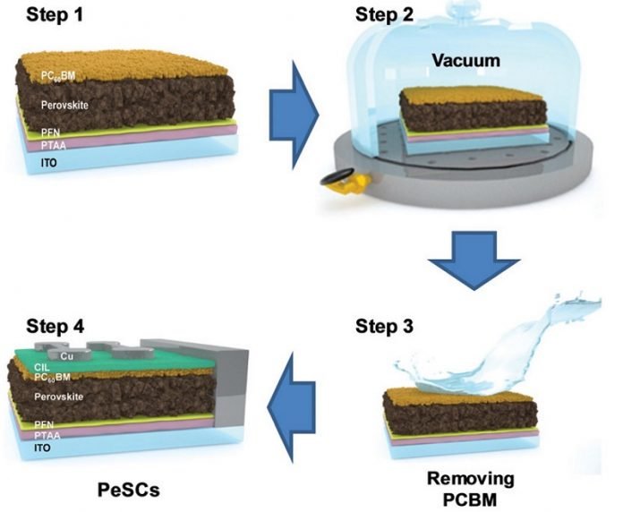
In this case, before putting the final electrode on top, the GIST scientists put the device in vacuum.
In prior experiments, the team had noticed that removing and then redepositing the top electrode and interlayer reduced burn-in loss, a rapid decrease in efficiency at the beginning of light illumination.
They subsequently confirmed that the high-vacuum environment used to deposit the electrode had contributed to this reduction. During vacuum curing, loose ions emerge from the perovskite and concentrate at the top interlayer.
In a second processing step, the scientists used a chemical solvent to selectively wash away this top layer.
“When these hybrid perovskites decompose, they start to leach negatively charged ions of iodine,” said lead author Hyungcheol Back, a research scientist at GIST and Hanwha Solutions.
“These ions can move around and accumulate at the interface between the active light-absorbing perovskite and metal electrode to form an insulating layer, making the device less conductive.”
With the developed processing protocol, the centimeter-size device maintained more than 80 percent of its initial efficiency (18.8 percent) under standard operational testing conditions of continuous illumination or heat (applied separately) for 1000 hours.
Moreover, the device did not exhibit burn-in loss, which is prevalent among hybrid perovskite solar cells.
To understand the improvement in stability, the GIST scientists performed characterization studies with process-modified and unmodified devices at the Center for Functional Nanomaterials (CFN) and National Synchrotron Light Source II (NSLS-II)—both U.S. Department of Energy (DOE) Office of Science User Facilities at Brookhaven National Laboratory.
At the Complex Materials Scattering (CMS) beamline, operated in partnership between CFN and NSLS-II, they conducted grazing-incidence wide-angle X-ray scattering experiments leveraging the CFN Advanced UV and X-ray Probes Facility.
In this technique, the X-ray beam grazes the sample at very shallow angles, which can be adjusted to probe the surface or bulk of a thin film at molecular length scales. According to the scattering patterns, the perovskite surface becomes more crystalline after loose ions are removed through the vacuum and solvent washing process.
To further confirm these results, the scientists performed X-ray photoemission spectroscopy depth profiling at the CFN Proximal Probes Facility.
The energy spectra of electrons ejected from the process-modified sample after it was irradiated with X-rays revealed that a smaller concentration of ions existed at the surface relative to the unmodified sample surface.
“The complementary tools at the CFN and NSLS-II allowed us to find out why the intrinsic stability of the material was enhanced,” said co-author Chang-Yong Nam, a materials scientist in the CFN Electronic Nanomaterials Group and an adjunct professor in the Department of Materials Science and Chemical Engineering at Stony Brook University.
“We should be able to apply this understanding to improve the performance of not only this material but also other hybrid perovskites, which share similar stability issues.”
Ultimately, the GIST team would like to apply their processing method to large-area (inch-size) device fabrication and develop engineering solutions for the commercial manufacturing of highly efficient large-area hybrid perovskite solar cells.
“Our results exemplify the type of synergy that a close international collaboration can create toward a scientific understanding critical to advancing important energy technologies like hybrid perovskite solar cells,” said Lee.
“The capabilities at the CFN and NSLS-II and the support received from scientists including Kevin Yager and Xiao Tong were instrumental. We look forward to future opportunities to conduct research at these user facilities.”


