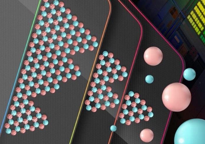
A small step for atoms, a giant leap for microelectronics.
Step by step, scientists are figuring out new ways to extend Moore’s Law.
The latest reveals a path toward integrated circuits with two-dimensional transistors.
A Rice University scientist and his collaborators in Taiwan and China reported in Nature today that they have successfully grown atom-thick sheets of hexagonal boron nitride (hBN) as two-inch diameter crystals across a wafer.
Surprisingly, they achieved the long-sought goal of making perfectly ordered crystals of hBN, a wide band gap semiconductor, by taking advantage of disorder among the meandering steps on a copper substrate.
The random steps keep the hBN in line.
Set into chips as a dielectric between layers of nanoscale transistors, wafer-scale hBN would excel in damping electron scattering and trapping that limit the efficiency of an integrated circuit.
But until now, nobody has been able to make perfectly ordered hBN crystals that are large enough — in this case, on a wafer — to be useful.
Brown School of Engineering materials theorist Boris Yakobson is co-lead scientist on the study with Lain-Jong (Lance) Li of the Taiwan Semiconductor Manufacturing Co. (TSMC) and his team.
Yakobson and Chih-Piao Chuu of TSMC performed theoretical analysis and first principles calculations to unravel the mechanisms of what their co-authors saw in experiments.
As a proof of concept for manufacturing, experimentalists at TSMC and Taiwan’s National Chiao Tung University grew a two-inch, 2D hBN film, transferred it to silicon and then placed a layer of field-effect transistors patterned onto 2D molybdenum disulfide atop the hBN.
“The main discovery in this work is that a monocrystal across a wafer can be achieved, and then they can move it,” Yakobson said. “Then they can make devices.”
“There is no existing method that can produce hBN monolayer dielectrics with extremely high reproducibility on a wafer, which is necessary for the electronics industry,” Li added. “This paper reveals the scientific reasons why we can achieve this.”
Yakobson hopes the technique may also apply broadly to other 2D materials, with some trial and error.
“I think the underlying physics is pretty general,” he said. “Boron nitride is a big-deal material for dielectrics, but many desirable 2D materials, like the 50 or so transition metal dichalcogenides, have the same issues with growth and transfer, and may benefit from what we discovered.”
In 1975, Intel’s Gordon Moore predicted that the number of transistors in an integrated circuit would double every two years. But as integrated circuit architectures get smaller, with circuit lines down to a few nanometers, the pace of progress has been hard to maintain.
The ability to stack 2D layers, each with millions of transistors, may overcome such limitations if they can be isolated from one other. Insulating hBN is a prime candidate for that purpose because of its wide band gap.
Despite having “hexagonal” in its name, monolayers of hBN as seen from above appear as a superposition of two distinct triangular lattices of boron and nitrogen atoms.
For the material to perform up to spec, hBN crystals must be perfect; that is, the triangles have to be connected and all point in the same direction. Non-perfect crystals have grain boundaries that degrade the material’s electronic properties.
For hBN to become perfect, its atoms have to precisely align with those on the substrate below. The researchers found that copper in a (111) arrangement — the number refers to how the crystal surface is oriented — does the job, but only after the copper is annealed at high temperature on a sapphire substrate and in the presence of hydrogen.
Annealing eliminates grain boundaries in the copper, leaving a single crystal. Such a perfect surface would, however, be “way too smooth” to enforce the hBN orientation, Yakobson said.
Yakobson reported on research last year to grow pristine borophene on silver (111), and also a theoretical prediction that copper can align hBN by virtue of the complementary steps on its surface.
The copper surface was vicinal — that is, slightly miscut to expose atomic steps between the expansive terraces. That paper caught the attention of industrial researchers in Taiwan, who approached the professor after a talk there last year.
“They said, ‘We read your paper,'” Yakobson recalled. “‘We see something strange in our experiments. Can we talk?’ That’s how it started.”
Informed by his earlier experience, Yakobson suggested that thermal fluctuations allow copper (111) to retain step-like terraces across its surface, even when its own grain boundaries are eliminated. The atoms in these meandering “steps” present just the right interfacial energies to bind and constrain hBN, which then grows in one direction while it attaches to the copper plane via the very weak van der Waals force.
“Every surface has steps, but in the prior work, the steps were on a hard-engineered vicinal surface, which means they all go down, or all up,” he said. “But on copper (111), the steps are up and down, by just an atom or two randomly, offered by the fundamental thermodynamics.”
Because of the copper’s orientation, the horizontal atomic planes are offset by a fraction to the lattice underneath. “The surface step-edges look the same, but they’re not exact mirror-twins,” Yakobson explained. “There’s a larger overlap with the layer below on one side than on the opposite.”
That makes the binding energies on each side of the copper plateau different by a minute 0.23 electron volts (per every quarter-nanometer of contact), which is enough to force docking hBN nuclei to grow in the same direction, he said.
The experimental team found the optimal copper thickness was 500 nanometers, enough to prevent its evaporation during hBN growth via chemical vapor deposition of ammonia borane on a copper (111)/sapphire substrate.
Written by Mike Williams.


