Discovery means simpler and cheaper manufacturing methods are actually beneficial for the material’s use in next-generation solar cells or LED lighting.
Scientists at the University of Cambridge studying perovskite materials for next generation solar cells and flexible LEDs have discovered that they can be more efficient when their chemical compositions are less ordered, vastly simplifying production processes and lowering cost.
The surprising findings, published in Nature Photonics, are the result of a collaborative project, led by Dr. Felix Deschler and Dr. Sam Stranks.
The most commonly used material for producing solar panels is crystalline silicon, but to achieve efficient energy conversion requires an expensive and time-consuming production process.
The silicon material needs to have a highly ordered wafer structure and is very sensitive to any impurities, such as dust, so has to be made in a clean room.
In the last decade, perovskite materials have emerged as promising alternatives.
The lead salts used to make them are much more abundant and cheaper to produce than crystalline silicon, and they can be prepared in a liquid ink that is simply printed to produce a film of the material.
The components used to make the perovskite can be changed to give the materials different colours and structural properties, for example making the films emit different colours or collect sunlight more efficiently.
You only need a very thin film of this perovskite material—around one thousand times thinner than a human hair—to achieve similar efficiencies to the silicon wafers currently used, opening up the possibility of incorporating them into windows or flexible, ultra-lightweight smartphone screens.
“This is the new class of semiconductors that could actually revolutionise all these technologies,” said Sascha Feldmann, a Ph.D. student at Cambridge’s Cavendish Laboratory.
“These materials show very efficient emission when you excite them with energy sources like light, or apply a voltage to run an LED.
“This is really useful but it remained unclear why these materials that we process in our labs so much more crudely than these clean-room, high-purity silicon wafers, are performing so well.”
Scientists had assumed that, like with silicon materials, the more ordered they could make the materials, the more efficient they would be. But Feldmann and her co-lead author Stuart MacPherson were surprised to find the opposite to be true.
“The discovery was a big surprise really,” said Deschler, who is now leading an Emmy-Noether research group at TU Munich. “We do a lot of spectroscopy to explore the working mechanisms of our materials, and were wondering why these really quite chemically messy films were performing so exceptionally well.”
“It was fascinating to see how much light we could get from these materials in a scenario where we’d expect them to be quite dark,” said MacPherson, a Ph.D. student in the Cavendish Laboratory.
“Perhaps we shouldn’t be surprised considering that perovskites have re-written the rule book on performance in the presence of defects and disorder.”
The researchers discovered that their rough, multi-component alloyed preparations were actually improving the efficiency of the materials by creating lots of areas with different compositions that could trap the energised charge carriers, either from sunlight in a solar cell, or an electrical current in an LED.
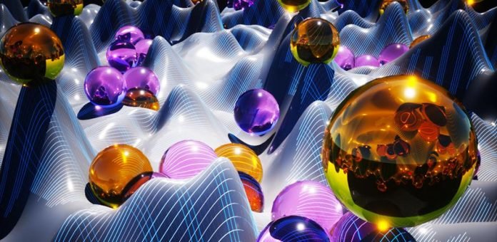
“It is actually because of this crude processing and subsequent de-mixing of the chemical components that you create these valleys and mountains in energy that charges can funnel down and concentrate in,” said Feldmann.
“This makes them easier to extract for your solar cell, and it’s more efficient to produce light from these hotspots in an LED.”
Their findings could have a huge impact on the manufacturing success of these materials.
“Companies looking to make bigger fabrication lines for perovskites have been trying to solve the problem of how to make the films more homogenous, but now we can show them that actually a simple inkjet printing process could do a better job,” said Feldmann.
“The beauty of the study really lies in the counterintuitive discovery that easy to make does not mean the material will be worse, but can actually be better.”
“It is now an exciting challenge to find fabrication conditions which create the optimum disorder in the materials to achieve maximum efficiency, while still retaining the structural properties needed for specific applications,” said Deschler.
“If we can learn to control the disorder even more precisely, we could expect further LED or solar cell performance improvements—and even push well beyond silicon with tailored tandem solar cells comprising two different colour perovskite layers that together can harvest even more power from the sun than one layer alone,” said Dr. Sam Stranks, University Lecturer in Energy at the Cambridge Department of Chemical Engineering and Biotechnology and the Cavendish Laboratory.
Another limitation of perovskite materials is their sensitivity to moisture, so the groups are also investigating ways to improve their stability.
“There’s still work to do to make them last on rooftops the way silicon can—but I’m optimistic,” said Stranks.


