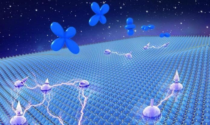
In a paper published in Nature, scientists at the University of California, Irvine and other institutions unveil a new process for producing oxide perovskite crystals in exquisitely flexible, free-standing layers.
A two-dimensional rendition of this substance is intriguing to scientists and engineers, because 2D materials have been shown to possess remarkable electronic properties, including high-temperature superconductivity.
Such compounds are prized as potential building blocks in multifunctional high-tech devices for energy and quantum computing, among other applications.
“Through our successful fabrication of ultrathin perovskite oxides down to the monolayer limit, we’ve created a new class of two-dimensional materials,” said co-author Xiaoqing Pan, professor of materials science & engineering and Henry Samueli Endowed Chair in Engineering at UCI.
“Since these crystals have strongly correlated effects, we anticipate they will exhibit qualities similar to graphene that will be foundational to next-generation energy and information technologies.”
For all of their promising physical and chemical properties, oxide perovskites are difficult to render in flat layers due to the clunky, strongly bonded structure of their crystals.
Earlier efforts at making free-standing, monolayer films of the material through the pulsed laser deposition method failed.
Pan’s cross-disciplinary group of researchers applied a technique called molecular beam epitaxy to grow the thin oxide films layer by layer on a template with a water-dissolvable buffer, followed by etching and transfer.
“Most of the known two-dimensional materials can be synthesized by exfoliation or by chemical deposition, as their bulk crystals consist of unique layered structures in which many strong covalently bonded planes are held together by weak van der Waals interactions,” he said.
“But oxide perovskite is different; like most oxide materials, it has strong chemical bonds in three dimensions, making it especially challenging to fabricate into two dimensions.”
Pan, who holds a dual appointment as a professor of physics & astronomy and directs the Irvine Materials Research Institute, said that molecular beam epitaxy is a more precise method for growing oxide perovskite thin films with almost no defects.
He knows this because his research team was able to review its work at atomic resolution using aberration-corrected transmission electron microscopy.
“TEM played a crucial role in this project, because it provided important feedback for the optimization of film growth conditions and allowed us to directly observe novel phenomena, including the crystal symmetry breaking and unexpected polarization enhancement under the reduced dimension,” Pan said.
“Given the outstanding physical and chemical properties of oxide perovskites and novel phenomena emergent at the monolayer limit, this work opens new possibilities in the exploration of quantum behaviors in strongly correlated two-dimensional materials,” he added.


